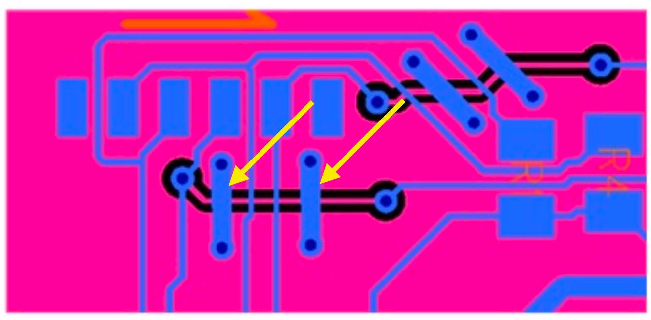
But my question is about Ground Planes. I was not able to reproduce Ground Planes on my previous etched PCBs. I am about to send of for new PCBs and my question is... should I leave dead areas of the the Ground Plane dead? I only connected the fields that had components that required grounding. Is there an advantage to connecting all of the fields to have a ground? Even if they are not used.
Actual PCB I am currently working to send off to be made.
Add ground plane to the bottom of a double sided PCB.
Avoid adding a ground plane (or copper pour) on the top/component side.
The bottom Ground plane should not be chopped up by traces; should be unobstructed.
Long cross unders should be strapped to the top or with bottom side zero ohm resistors.
Thanks for the reply Larry. I have been using wide traces to connect my areas that need grounds. But, I was concerned about the areas that aren't glowing in my active "ground" area on my above image.
Should I connect them all to be active grounds?
Is my yes or no question answered somewhere in that hour and half video?
Imagine I am making a PCB with SMD components with vias to the "bottom" ground plane... I have some dead areas that that aren't connected to the rest of the ground plane.
Should I be concerned with connecting the areas that do not have components to be connected?
There should be no islands of unconnected copper in the bottom GND plane.
Avoid long cross under traces, these result in long GND return paths.
If you have such traces, they should be appropriately strapped so GND return signals can get past such bottom traces. Get these traces to the top as soon as you can. Don’t cut up your GND plane.
With regards to breaking up a ground pour with traces that cut through it. It is basic electronics that in order to minimise both the generation of electrical noise and picking up noise and interference the 2 conductors carrying an electrical signal from source to destination must be kept physically close to each other, this is why twisted pairs are useful for carrying signals long distances with minimal interference. This rule is just as important with a PCB. On a PCB the signal will typically be on a trace on the top layer and its return path through the ground plane underneath. As the ground plane covers all the PCB it's easy to forget that the return path for a signal still needs to be close to the signal path, which means that there should be unbroken copper on the ground plane directly below every signal path. Anything that breaks that will introduce noise and increase EMI emissions. The next question is whether it really matters in your circuit. Well it doesn't matter for flashing an LED, but it matters at 100MHz. As digital circuits operate with square waves and square waves have lots of harmonics then it's safest to assume there will be relevant frequencies in most microcontroller projects. Take @LarryD 's advice seriously.
What CAD software are you using?
Some will alert you to the fact that you have isolated islands (dead area) and you have the option of keeping them or removing them.
Don't get TOO hung up on "best practices."
An Arduino-like board doesn't feature power-hungry chips with multiple power rails and GHz clocks, and has a lot of leeway.
Several official Arduino boards have been cited as "bad examples" of PCB design, and yet the number of problems reported anywhere that can be traced to those flaws is minimal (I don't think I've seen ANY...)
"dead areas" are common on mechanically routed boards, and likewise don't usually seem to create problems.
Two layer boards from the dawn of hobby computing, with no grounds planes at all, have worked fine.
Wire wrap, stripboard, and free-form wired versions of Arduino and arduino-like circuits work fine, too.
At last......
I have been following this thread with ever-increasing trepidation, but all I want is something neater, and easier to solder, than the usual rats nest on a proto shield.