Hello everyone, I am a newbie and I am intending to design a PCB of a mosfet driver for a solenoid.
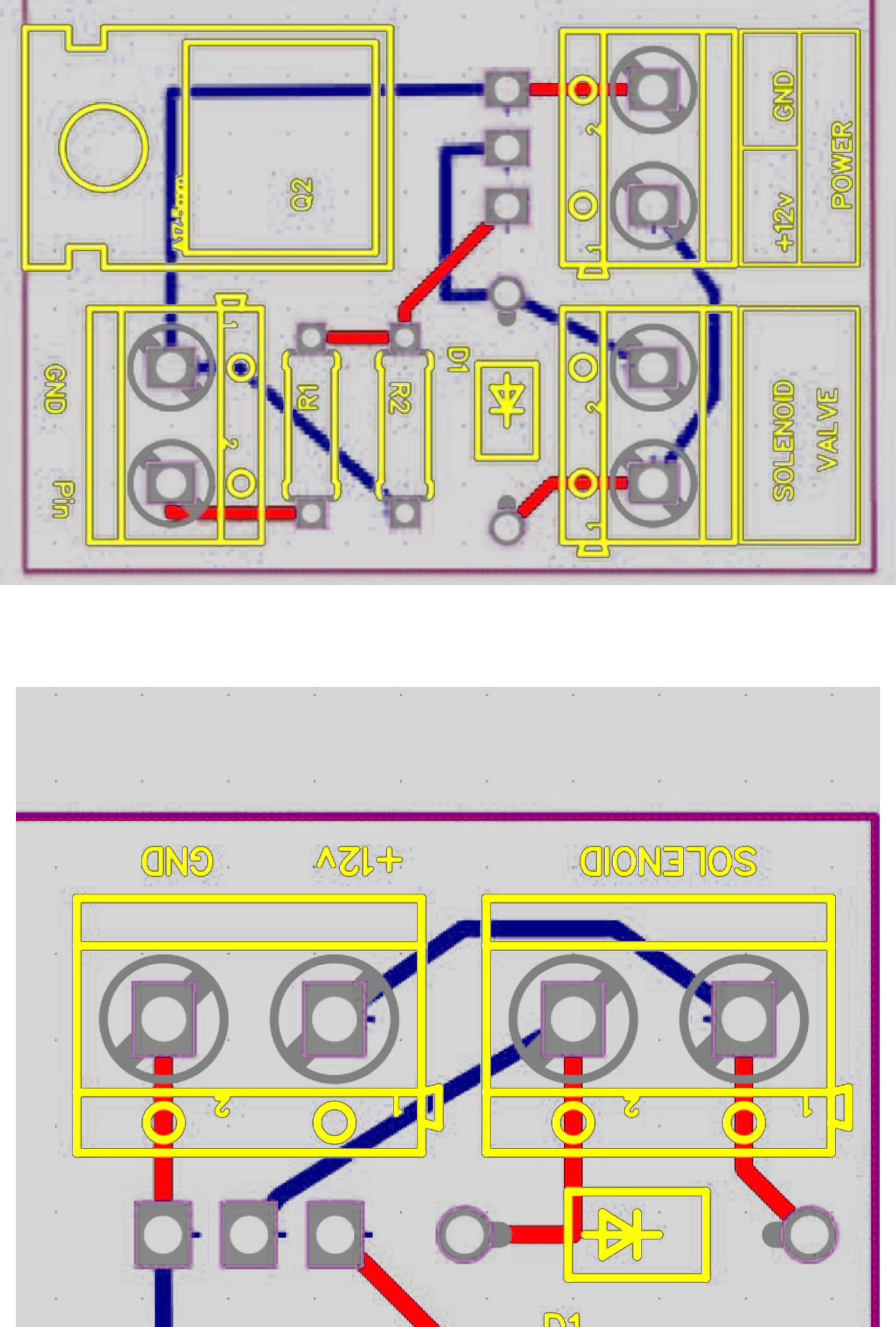
I have a doubt with the wiring of the flyback diode. In the first image you can see the complete PCB where you can observe my last version of the wiring for the diode. The second image is a detail of the first version i did for the diode wiring.
You only have one crossing of traces so it would be easy to make this a single-sided board. It would be easier to debug if all of the traces were on the bottom.
Thank you for your swift answer. I understand, it is easy to arrange.
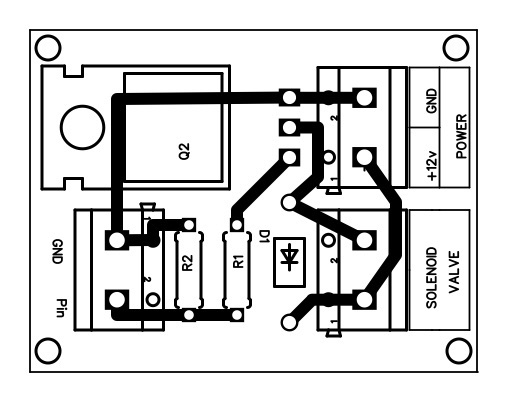
What is your opinion about the diode wiring. I guess that the second image is wrong but ...
Thank you @PerryBebbington. I have already made the tracks wider.
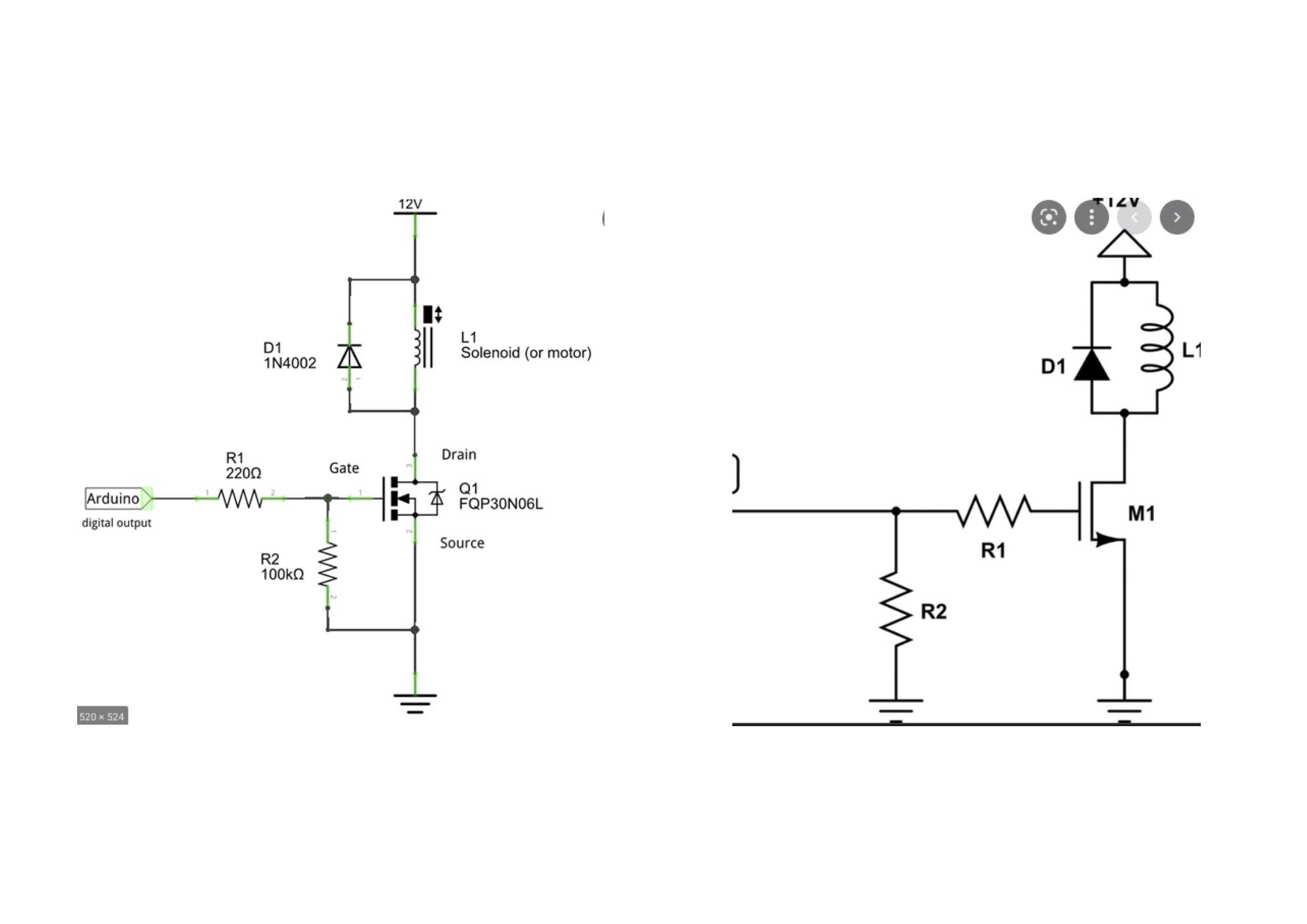
Concerning R2 and R1. R1 is for me 220Ohms and R2 10K. WHen I started I found a lot of projects and examples and I found 2 different versions respect the placement of the resistors. Like in the picture below.
I appreciate your remark about it.
Use the second one, the one where R1 and R2 don't form a divider. Yes, I agree that with those resistor values it makes hardly any difference, but it's good practice and a good habit to get in to. In any case, it's practice in thinking about what you are doing and why.
So, do it because you understand why, not because I (or anyone else) told you to do it that way.
Thank you @cncnotes, yes, I am using a logic level mosfet, IRL Z 44N.
You are of course right @PerryBebbington and I am trying to learn. I understood bad the voltage divider circuit, in concrete I interpreted it in the other way round, I understood that if I place R2 at the left of R1 I was creating a voltage divider. Now I understood.
Thank you all
Thank you Paul_B.
As I said in my first post I am newbie and I would like really to learn and do the things right.
I will appreciate a lot if you please can clarify to me what is wrong with the diode and the missing decoupler capacitor.
Thank you on advance.
Briefly put, people get confused as to what happens when the FET switches off.
The matter of the "flyback" or whatever you call it is that the current in the inductor then instantaneously keeps flowing - but declines exponentially.
So all the current which was supplied by the FET, is now flowing through the diode. The current through the coil does not suddenly stop - as said, it declines exponentially.
What does happen is that the current being drawn from the supply does stop very suddenly. So that sudden current impulse in the wires (including the ground wire) to the supply can be coupled as an inductive impulse, to other parts of your wiring which (particularly the microcontroller circuitry) may be sensitive to such impulses.
And if the ground connection is common to other parts of the circuit, the sudden change in voltage drop due to the step in current may also affect those other parts.
People fail to understand that this impulse is in the supply wiring, not in the wiring to the inductor unless you mount the diode at the inductor. The part of the wiring between diode and inductor does not experience a current impulse, only the wiring between the diode, the FET and the supply.
So to limit the extent of that current impulse, you need a capacitor of decent size (470 µF or 1 mF would be a good start) directly across the FET and diode to absorb the current impulse and keep it out of the wiring back to the supply. The circuit that needs to be kept as physically small as possible to contain the impulse is the "triangle" of the FET, the diode and that capacitor.
I really appreciate that you have not been brief. Thank you a lot.
I was one of the people who "fail to understand that this impulse is in the supply wiring, not in the wiring to the inductor".
I guess I understood (I hope).
Below is the design with the addition of the capacitor.