I just try to have constant input for zero crossing detection.The rest of the schematic is the same like the last (We agree for this) I order MOSFET N-chanel XFQ50N60P3 (600V, 50A) .My input to rectifier bridge will be steel variable from 100 to 150V max . Voltage for L1 is variable from 50 to 75V max. I will go slow from starting value for the voltage to the max to see if I will have the reaction I expect from the two coils L1 and L2. Because my limit for L1 load is set to 75V AC. Other way I will have overheating.
From what I observe it is no difference if I stick to original zero cross detection or I use another transformer for zero cross detection. I just worry the ARDUINO board will not recognized this drop of input voltage on pin2 , because it do not drop to 0V
Everything else is ready for the test, but I have to wait to receive the Mosfet I ordered.
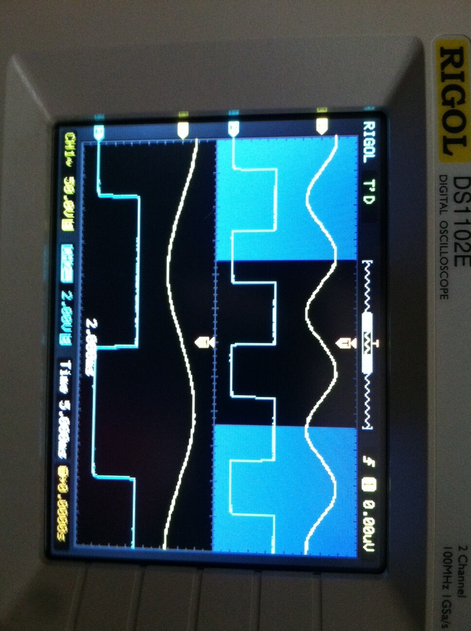
Is this is a problem what I observe on my oscilloscope or it will work?
That scope signal doesn't make sense AT ALL for this circuit - assuming you indeed built the circuit exactly as the schematic drawing you posted.
The signal should make peaks at the transitions. It looks like one of the two diodes is blown, so there's light produced only for one half of the wave pulling the signal low (but apparently not completely), and the other half of the time the signal is pulled high as there is no light produced by the LED at all, and the transistor blocks.
The 8.3 ms you mention is what you expect for a half wave of a 60 Hz signal.
What voltage do you see when you connect the scope to the input pins of the H11AA1?
Hi,
Can you post a picture of your setup of the H11AA1 and the connection to the scope please.
I agree with #wvmarle it looks like one of the diodes in the opto has failed.
It is really a H11AA1 as that is the sort of output you would get from a standard single LED input opto?
That's another thing indeed: the low level should be zero but is about 1/2 Vcc. That's not good either, and implying either the H11AA1 is defective, or there's another error in the circuit.
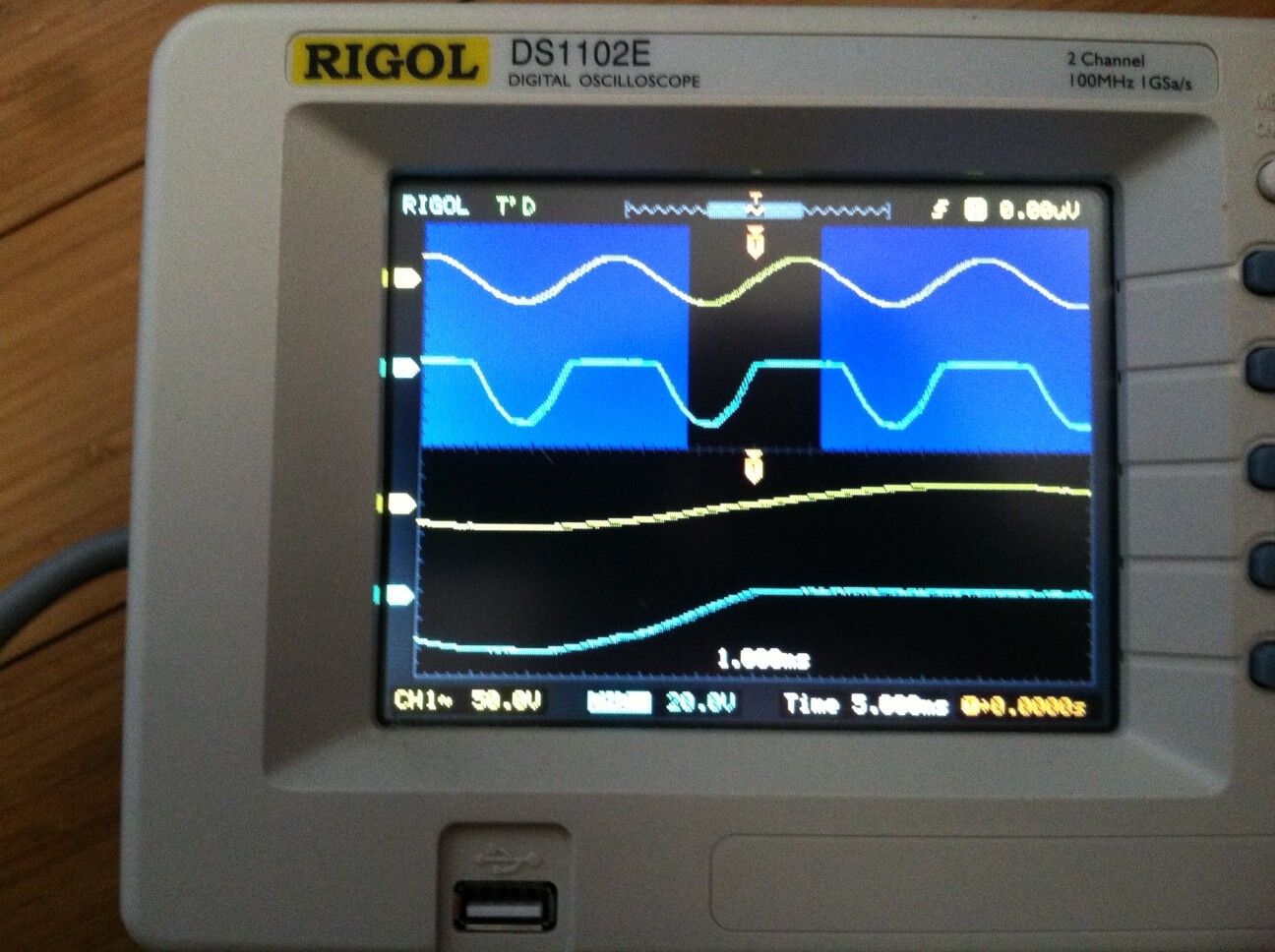
I change the H11AA1 again and now I have half wave +5V and half wave +0V. I think remarks of "cattledog" (If you can get the output voltage levels correct, you could use the device you have with a CHANGE interrupt, and pick up the zero crossings), are good and instead( attachinterrupt, RISING)to use CHANGE. See attached photo of my oscilloscope with final reading.Now it is no matter what voltage I use the readings are the same only difference is the resistors in the input of H11AA1 (at 150V max , R=15K) and(at 24V, R=2.2K). May be with constant input of 24V is more safe for the optocoupler.
Yes, they are exact from zero cross to zero cross . Sorry I forgot to attach picture of voltage between pin 1 and pin 2 of H11AA1.Now I correct this -see the picture
It certainly looks like you have an H11A1 instead of an H11AA1. One is single channel and the other is double.
Are those two halves equal length? It looks a bit different to me.
Yes. With the single sided device, the transitions will be offset from actual zero by some amount relating to the threshold current required to illuminate the input led.
You may need to read the state of the input when the CHANGE interrupt triggers, and adjust the triac firing delay times accordingly.
Hi,
17Vac is way too high, it should be lower like 1.5Vac., due to the clamping of the 27Vac by the back to back diodes.
What is your series resistor value between the AC supply and the opto input?
Does your DMM have DIODE test, if so put it in that mode and tell us the readings between pin1 and pin2 in both directions of the test leads, you will need to take the opto out of circuit to test.
(38 - 1.071)/2200 = 0.016A = 16mApk or 11mArms within spec for opto.
How are you connecting your scope to the circuit?
Where are you connecting the probe gnds to?
What do you see on the scope if all you have connected is one channel between pin4/gnd and pin5/signal of the opto?
Completely disconnect the other channel.
Voltage now between pin1 and pin2 is 1.2V and I have short +5V picks on my oscilloscope. You are genius Tom!!! Why is this so confusing when I monitoring input wave?
Hi,
Your scope probes, the gnd on each is connected together at the scope.
So when you were monitoring the input and the output of the opto, the gnds from each channel were connecting the input and the output of the opto.
So it defeated the isolation you needed to be able to see full AC at the opto input.
Thank you TomGeorge , now I understand why I lost a year trying to use different components MOSFET, TRIAC,BTA,LGBT and never get the result for output I was looking. Plus I was using program codes for different schematics I found at different sources, not my own ,because I do not know how to program ARDUINO.
Now I am ready to build the schematic I like mostly (Dec 09, 2017, 02:26 pm Last Edit: Dec 09, 2017, 02:27 pm by wvmarle) . Can you help me, all of you, to write Program code specific for this schematic. You work very hard to educate me and I am very very thankful.
With that schematic a concern is the value of R5.
What is the voltage range for this part of the circuit? I've seen so many it's confusing (it should be a good value for 100-150V input range).
Gate to emitter voltage has to be in range 30 >V(ge)>3 . I think R5 and R6 acting like voltage divider and to lover 150V DC with picks of 210V to range of 8to20v ( if R6 is 220k -R5 has to be 260kOhm) Or may be I am wrong? I have no idea how to include R3 andR4 in this calculation.