UNO R3: Internal Architecture of Timer/Counter Module of ATmega328P MCU

1.
The diagram of Fig-1 is posted for the readers looking for a brief architecture of the TImer/Counter Module of the MCU of UNO R3 Board. Feedbcak is welcome to improve the diagram.


Figure-1:

2.
Preset Count Concept (TC1)


fullCount = presetCount + actualCount
Figure-2:

3.
Normal Mode Operation of TC1
In Normal Mode Operation the counter keeps counting in te upward direction, and it simply overruns when passes its maximum 16-bit value (MAX = 0xFFFF) and then restarts from the BOTTOM (0x0000) or forced preset count.

If interrupt enable bits are active, then there can be three interrupt points in a single counting process (Fig-3).


Figure-3.

4
Testing the Interrupts of Fig-3 (for TC1)


Figure-4:

Sketch: (not tested)

volatile bool flagV;
volatile bool flagfa;
volatile bool flagfb;

void setup()
{
  Serial.begin(9600);
  pinMode(13, OUTPUT);
  pinMode(12, OUTPUT);
  pinMode(11, OUTPUT);
  pinMode(2, INPUT_PULLUP);
  TCCR1A = 0;
  TCCR1B = 0;
  TCNT1 = 3036; //preset count
  OCR1A = 18661;
  OCR1B = 49911;
  TIMSK1 |= (1 << TOIE1) | (1 << OCIE1A) | (1 << OCIE1B);
  while (digitalRead(2) != LOW)
  {
    ;  //wait until K1 is pressed
  }
  TCCR1B = 0x05;  //start TC1 with division factor 1024
}

void loop()
{
  if (flagV == true)
  {
    digitalWrite(13, HIGH);
    delay(200);
    digitalWrite(13, LOW);
    delay(200);
    flagV = false;
  }

  if (flagfa == true)
  {
    digitalWrite(11, HIGH);
    delay(200);
    digitalWrite(11, LOW);
    delay(200);
    flagfa = false;
  }

  if (flagfb == true)
  {
    digitalWrite(12, HIGH);
    delay(200);
    digitalWrite(12, LOW);
    delay(200);
    flagfb = false;
  }

}

ISR(TIMER1_OVF_vect)
{
  TCNT1 = 3036;  //preset count
  flagV = true;
}

ISR(TIMER1_COMPA_vect)  //comparison is made with the content of OCR1A Register
{
  flagfa = true;
}

ISR(TIMER1_COMPB_vect)  //comparison is made with the content of OCR1B Register
{
  flagfb = true;
}

5.
Clear Timer on Compare Match (CTC- 4) Mode Operation to Generate Square Wave Signal at DPin-9 (for TC1)
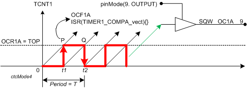

Figure-5:

Working Principle: When CTC Mode 4 is selected (WGM[13:10] = {0,1,0,0}, COM1A[1:0] = {0,1}, and pinMode(9, OUTPUT)), the Timer/Counter1 (TC1) hardware is configured to count upward from 0 and continuously compare the count value with the content of the OCR1A register (Fig-5). The value loaded into the OCR1A register is referred to as TOP, which represents the highest count value reached by TC1 before the counter is cleared and restarted in this mode of operation.

Whenever a compare match occurs at points P, Q, and so on, the logic state of digital pin 9 (OC1A) toggles. Consequently, a square wave is generated on pin 9, with its frequency determined by the following formula. The output frequency can be adjusted by changing the value stored in the OCR1A register.

f =  clkSYS/(2*N*(1+OCR1A))  
where: N=TC1 Clock Prescaler (1,8,64,256,or 1024),clkSYS=16 MHz


Figure-6:

Sketch: (to genertae 1 Hz square wave)

void setup()
{
  Serial.begin(9600);
  pinMode(9, OUTPUT);//DPin-9 (OC1B signal/pin must be set as output)
  
  TCCR1A = 0x00;  //reset register
  TCCR1B = 0x00;
  TCCR1B |= bit(WGM12); //1<<WGM12  ; Mode-4 TOP = OCR1A
  TCCR1A |= bit(COM1A0) | bit(COM1B0); //toggle at DPin-9;
  TCNT1 = 0x0000;
  OCR1A = 31249;//1 Hz signal
  TCCR1B |= bit(CS12); //start TC1 with clkcTC1 = 16 MHz/256 = 62500
}

void loop()
{

}

6.
Generation of Fast PWM Signal in Mode-14 Operation of TC1 (single slope)
Fast PWM signal refers to “high frequency” PWM signal; where, frequency can be varied from 1 Hz to 8 MHz by changing the values of N (TC1 clock prescaler) and ICR1 Register and the duty cycle is regulated for Ch-A by changing the value of OCR1A Register (Fig-7).

f = sysClk/(N*(1+ICR1))
==> (16 000 000)/(N*(1+ICR1))
==>  (16 000 000)/(N*(1+TOP)); 
where:N=1,8,64,256,1024


Figure-7:

Working Principles: In Fig-7, TC1 starts counting up from BOTTOM (= 0). Frequency of the driving clock is: clkTC1 (= clckSYS/N). In non-invert mode, initially DPin-9 (OC1A) is at HIGH state and then goes to LOW state at Point-P when TC1 becomes equal to OCR1A. TC1 keeps counting up and when it becomes equal to ICR1 at Point-R, DPin-9 assumes HIGH state. As a result, there generates one cycle of the PWM signal. At Point-R, TC1 is reset to zero and begins to count up again.

Sketch: (to genertae 1 Hz signal)

  • Connect RLED with DPin-9 to monitor PWM signal.
  • Reset TCCR1A and TCCR1B Registers
  • Select Mode-14 for Fast PWM
  • Select non-inverting mode for PWM signal for Ch-A
  • Compute value for ICR1 for 1 Hz using a suitable N = 256 (clkTC1 prescaler)
  • Load 50% duty cycle value in OCR1A
  • Start TC1 with N = 256
  • Check that RLED is blinking at 1 Hz.

Codes for the above tasks:

#define OC1A 9
 
void setup()
{
  Serial.begin(9600);
  pinMode(OC1A, OUTPUT); //Ch-A
  TCCR1A = 0x00;   //reset                              
  TCCR1B = 0x00;   //TC1 reset and OFF         
  //fOC1A/B = clckSys/(N\*(1+ICR1); Mode-14 FPWM; OCR1A controls duty cycle
  // 1 Hz = 16000000/(256\*(1+ICR1) N=1,8,64,256,1024 ==> ICR1 = 62500
  TCCR1A |= (1 << WGM11); //Mode-14 Fast PWM           
  TCCR1B |= (1 << WGM13) | (1 << WGM12);        //Mode-14 Fast PWM      
  TCCR1A |= (1 << COM1A1) | (0 << COM1A0);//Non-invert:HIGH-LOW at COMPA match 
  ICR1 = 62499;   // TOP for 1Hz frequency
  OCR1A = 31250;  //= 50% duty cycle
  TCNT1 = 0;
  TCCR1B |= (1 << CS12);//TC1 start with N = 256; clkTC1 = 62500; 
}

void loop()
{
 
}

7.
Changing duty cycle and frequency of Fig-7
In Fig-7, it is observed that the duty cycle of the PWM signal can be changed by shifting the position of Point-Q which depends on the content of OCR1A Register. Likewise, the frequency can be changed by changing the content of ICR1 Register, which shifts the position of Point-R.

In Fig-8, the content of OCR1A register will be changed by rotating Pot1 which feeds changing voltage to Ch-0 of the ADC. Likewise, the content of ICR1 register will be changed by rotating Pot2 which feeds changing voltage to Ch-1 of the ADC.


Figure-8:

The duty cycle and frequency of the PWM signal can be changed in the loop() function by including the following codes.

OCR1A = map(analogRead(A0), 0, 1023, 0,  62500);  //duty cycle: 0% to 100%

The value of OCR1A can also be loaded at time Point-P (Fig-7) when there occurs an interrupt due to Compare Match – A event. The codes are:

bitSet(TIMSK1, OCIE1A);  //COMPA interrupt is enabled 
ISR(TIMER1_COMPA_vect)
{
    OCR1A = map(analogRead(A0), 0, 1023, 0,  62500);  //duty cycle: 0% to 100%
}

The value of ICR1 Register can also be loaded at time Point-R(Fig-7) when there occurs an interrupt due to Capture Match. The codes are:

bitSet(TIMSK1, ICIE1);  //Input Capture interrupt logic is enabled Fig-11.12
ISR(TIMER1_CAPT_vect)
{
    ICR1 = map(analogRead(A1), 0, 1023, 62499, 1);  //f = 1 Hz to 31250 Hz
}

TOP is defined as the highest value in the count sequence at which compare match occurs and the counter value is either reset to zero (Fg-7).

The name Single Slope (Fig-7) conversion has come from the fact that the TC1 is only counting up along the positive slope and there is no counting down.

Resolution refers to the minimum amount of time by which the duty cycle of a PWM signal can be changed. For example: consider 1 Hz signal for Fig-7. With N=256, the TOP = 62499. Hence, the resolution is 1/62500 = 16 µs (= log (TOP + 1)/log (2) = 4.8/0.30 = 16 µs).

8.
Phase Correct PWM Signal in Mode-10 Operation of TC1 (dual slope)

f = sysClk/(2*N*ICR1)
==> (16 000 000)/(2*N*ICR1)
==> (16 000 000)/(2*N*TOP)); 
where:N=1,8,64,256,1024;TOP=ICR1,OCR1A

In Mode 10, the Phase Correct PWM mode generates a PWM signal whose frequency can be adjusted over a wide range by changing the Timer/Counter1 (TC1) clock prescaler (N) and the value stored in the ICR1 register. The duty cycle of Channel A is controlled by changing the value of the OCR1A register. The term Phase Correct indicates that the PWM outputs on Channels A and B are generated symmetrically with respect to the timer count, resulting in closely aligned signal phases and reduced timing skew between the channels.


Figure-9:

Working Principle: Referring to Fig-9, TC1 begins counting upward from Point A. The timer is driven by the clock clkTC1 (= clkSYS/N, as shown in Fig-8). In non-inverting mode, DPin-9 (OC1A) is initially in the HIGH state. When the TC1 count becomes equal to OCR1A at Point B, OC1A transitions to the LOW state.

The timer continues counting upward until it reaches the value stored in ICR1 at Point C. At this point, counting direction reverses and TC1 begins counting downward. When the count becomes equal to OCR1A at Point D, OC1A returns to HIGH state and remains HIGH until Point E.

Consequently, one complete PWM cycle is generated over the interval A–B–C–D–E. TC1 continues counting downward until it reaches zero at Point E. The timer then resumes upward counting and initiates the next PWM cycle.

The status flags OCF1A, OCF1B (not shown), ICF1, and TOV1 are automatically set at Points B, the OCR1B compare-match point, C, and E, respectively.

... in progress

Feedback is spelled incorrectly.

The diagram of Figure-1 ....

to improve

Have a look at the site below, one of the most elaborated sites about the 328 and programming MCU.

In Figure 1:

OC2FA / OC2FB should be FOC2A / FOC2B

What is PWM0A up to PWM2B?

Typo mistakes are corrected.

That is an excellent way of Gammon presentation that does not contain diagram of Fig-1 of post #1.

Typo mistakes:
OC2FA
==> OCF2A : compare Output Flag for Ch-A of TC2

OC2FB
==> OCF2B

FOC2A/B and OCF2A/B are both correct and different things (Fig-1).


Figure-1:

PWM0A ==> PWM signal of Ch-A of TC0
....................................................................
PWM2B ==> PWM signal of Ch-B of TC2

I have submitted the following digaram (Fig-1) to ChatGPT and have asked him/her as to what knowledge he/she would infer from the diagram: Please read his/her answer and give a rating to ChatGPT out-of-10, which is virtually a recognition to human efforts that have raised machine to think at such a high level.


Figure-1:

His/her answer:
From this block diagram, I infer that it represents the internal architecture of Timer/Counter1 (TC1) of the ATmega328P (used on the Arduino Uno R3). The diagram highlights how the timer, compare units, interrupt logic, and output pins interact.

Please, give your rating to ChatGPT out-of-10.

Key observations

1. TC1 is a 16-bit timer/counter

  • The register TCNT1 is shown as a 16-bit register (bits 15...0).
  • It can operate either as:
    • a timer driven by the internal clock (clkTC1), or
    • a counter driven by an external signal on T1 (PD5, Arduino D5).

2. Prescaler selection

The timer clock can be selected from:

  • Stop
  • ÷1
  • ÷8
  • ÷64
  • ÷256
  • ÷1024
  • External clock

This means the count rate can be adjusted by selecting the appropriate prescaler.

3. Two independent compare channels

TC1 contains:

  • OCR1A (Output Compare Register A)
  • OCR1B (Output Compare Register B)

The contents of TCNT1 are continuously compared with these registers.

When:

TCNT1 == OCR1A

the OCF1A flag is set.

When:

TCNT1 == OCR1B

the OCF1B flag is set.

4. Hardware waveform generation

The compare-match signals feed the waveform-generation hardware labeled:

  • PWM1A
  • PWM1B

This indicates that the timer can generate output waveforms entirely in hardware without CPU intervention.

5. Dedicated output pins

The waveform outputs appear on:

Channel MCU Pin Arduino Pin
OC1A PB1 D9
OC1B PB2 D10

Thus, Timer1 can directly control D9 and D10.

6. Interrupt generation

Each compare channel has its own interrupt path.

For Compare A:

ISR(TIMER1_COMPA_vect)

For Compare B:

ISR(TIMER1_COMPB_vect)

The interrupt occurs only if:

  • the local enable bit (OCIE1A or OCIE1B) is set, and
  • the global interrupt enable bit is set.

7. Overflow interrupt

When TCNT1 rolls over:

0xFFFF → 0x0000

the TOV1 flag is set.

If TOIE1 is enabled, the processor executes:

ISR(TIMER1_OVF_vect)

8. ICR1 is involved in advanced modes

The register ICR1 is shown connected to the compare logic. This suggests that in some modes:

  • ICR1 can act as the TOP value,
  • enabling variable-period PWM generation (such as Fast PWM Mode 14).

Important conceptual conclusion

The diagram shows that Timer1 is much more than a counter. It contains:

  1. A 16-bit counting unit.
  2. Two hardware comparators (A and B).
  3. Two waveform-generation channels.
  4. Three interrupt sources:
    *
    Compare A
    *
    Compare B
    *
    Overflow
  5. Direct hardware connections to output pins D9 and D10.

This explains why Timer1 can generate highly accurate square waves and PWM signals without requiring continuous CPU involvement. The CPU only needs to configure the registers; the hardware then performs the timing and waveform generation autonomously.

ZERO

How did it know it was a 328P and how did it know it was on an Uno R3 unless you did not tell it so.

1.
That poor fellow did a lot of hard work to align the symbolic names of my diagram with the real registers of 328P MCU; whereas, you being a veteran forum member had rated him/her with ZERO -- I think justice was not done to him/her!

2.
But the following statement of ChatGPT is correct; so, he/she must be given at least 1.

7. Overflow interrupt

When TCNT1 rolls over:

0xFFFF → 0x0000

the TOV1 flag is set.

If TOIE1 is enabled, the processor executes:

ISR(TIMER1_OVF_vect)

3.

It could be that he/she searched my post (here or in its server) and looked into the title. You may tell better how ChatGPT works.

4.
Do you want to say that the following line is incorrect?

When TCNT1 rolls over:
0xFFFF → 0x0000

Do you think it’s more understandable to treat all the timers together, rather than separating them by type? (All three timers on the 328 have unique features. And the newer AVRs more carefully name them like “timer type a” through “timer type f” (?), plus the RTC and PIT, plus maybe also a sysTick, generally with more serious differences.

Other architectures have even more types of timer, sometimes including a dedicated PWM module…

That I am leaving to the readers.

I hope that you will ack my manual labor of 2/3 hours spent to create the summary diagram of Fig-1 of post #1. The original purpose of this diagram was to present it through projector to my EEE-3/1 students and learning the features of the timers/counters in an interactive fashion. For example:

I ask them to find the possible values of clkTC1 when driving clock comes from internal oscillator.

And etc.

I still give it ZERO as that diagram could be for just about any AVR or ATtiny processor that has a 16 bit timer and has nothing to do with any Uno.

@jim-p
Then why did he/she align the given diagram with my TC diagram, which was specifically tied to the 328P? How was my intended meaning inferred? If my unstated intention was interpreted correctly, it raises the question of why penalty was assigned?

That is what I'm questioning?

Now, I see your point! I am impressed to see your meticulous observation.

Could it be that that my question to ChatGPT was right, but it has not been reflected in the opening paragraph of my post #8?

==>
I have submitted the following partial diagram (Fig-1) to ChatGPT after taking it from the full TC diagram of ATmega328P of UNO R3 board and have asked him/her as to what knowledge he/she would infer from the diagram:


Figure-1:

I always admire the diagrams you create.

If you haven't already done so, you might consider sharing (in a dedicated forum topic) the techniques and tools you use to create such diagrams. The shared knowledge would be useful to others hoping to achieve such results.

I think you raise a good criticism of the LLM's methods. I have noticed their general tendency to immediately provide answers based on unstated assumptions. If I had been asked the question in isolation, I would request clarification before proceeding. Some might argue that, for a machine, it is better to just go ahead and provide an answer, prefaced by a clear statement of its assumptions. However, I would still prefer that it only provide an answer once it has collected all the required information (or been informed by the user that the information is not available).

From the perspective of designing a mass market consumer product (which was the key to the initial success of ChatGPT), it probably does make sense to train the LLM in a manner that produces immediate results, even if that comes at the cost of accuracy. However, I don't think that approach is appropriate for our purposes.

I performed an experiment with the GitHub Copilot service where I asked it to recommend classification labels to apply to the issues in a GitHub repository's issue tracker. I clearly and explicitly specified that it must limit itself to the predefined set of labels from the repository's configuration. I happened to be watching the little "thinking" messages that indicate the agents progress and saw that it went out and downloaded a label configuration file from a separate repository. That made no sense, as there was no guarantee the list of labels specified in that file would be the same as the list specified in the target repository's configuration. On investigation, I found that the agent didn't have the permissions required for it to access the list of labels in the target repository, so it simply improvised by grabbing a likely list from another arbitrary source. It then soldiered on to provide me with a list of the labels it recommended applying. It did not make any mention that it had deviated from my instructions.

Even though I would not be surprised if the LLM simply guessed that the diagram was about the most common AVR chip, there is an alternative possibility: that @GolamMostafa did provide the information via context. ChatGPT (and other such services) utilizes context. This means the information the user provided earlier in a chat session will be considered when responding to later prompts in that session.

Thank you for the good words.

To be frank, the diagram comes from my understanding of the processor's architecture and is created manually using Microsoft Visio to draw lines, boxes. etc. and adding the text elements.

It is a labor-intensive task, and many people may not be willing to undertake it unless they genuinely enjoy doing this kind of work.

or from cookies or browser cache

I gave @GolamMostafa diagram to chat and it did mention the 328P and Uno R3. After I closed my browser, cleared cookies and cache, the same question only mentioned the 328P
Anyway enough AI for me.

Someone told me that the AI I was chatting with resides on a remote server and that all of my messages are instantly stored there. Therefore, according to that explanation, all responses come from the remote server.

If that is the case, why are you referring to cookies and browser cache, which are stored locally on PC?