for a little phone project i am now shrinking my breadboard set-up to a PCB with an ATmega328 chip.
The system will be powered by a 3.7V LiPo battery. I've used the official Arduino Nano schematics for the ATmega328 itself and the charging circuit was put together through different posts in this forum and others.
Would anyone be so kind to quickly review it, if there is something major i overlooked?
I'm planning to burn the bootloader with an external ISP programmer as well as TQFP32 socket before soldering it to the PCB. And then do the regualr programming via USB.
It looks like he already has everything discussed in the video. I think the circuit looks fine, but I haven't really checked the DW01 stuff. But it just needs to be like the circuit in the datasheet.
Edit: Forgot to say - you show the Atmega328PB. That's not the same as the Atmega328P used in the Nano.
My SIM A760E module needs between 3.4V - 4.2V voltage supply, which is perfect for directly driving it from my 3.7V LiPo.
Problem is, i also want it to be active when connected to the USB (e.g. while charging).
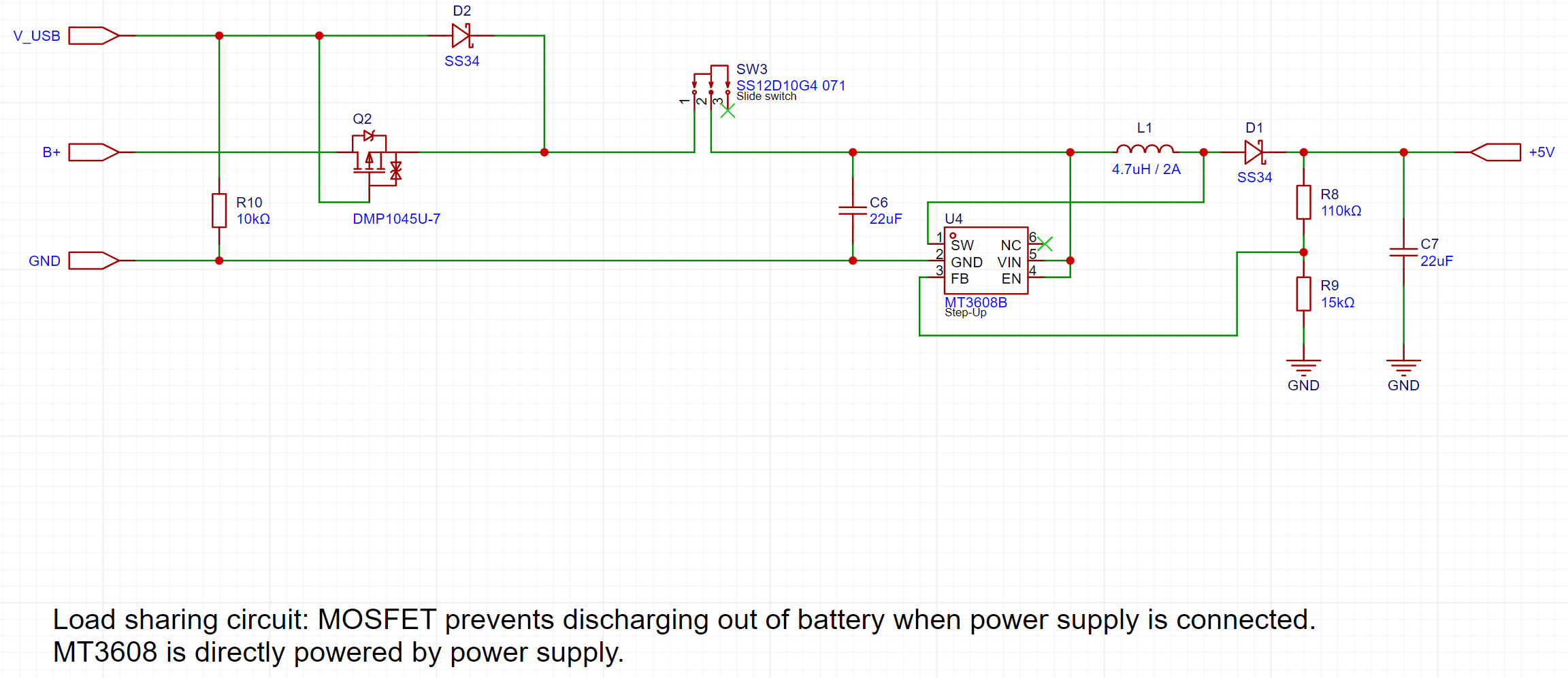
So the solution was to step-down the 5V USB to 4.1V, which is done by the LDO as seen below.
Unfortunately, with my load sharing circuit, i haven't found a fitting solution to automatically switch between the battery voltage B+ (when USB is not connected) and the generated +4.1V (when USB is connected).
I could just put the LDO behind the 5V step-up, but that would result in unnecessary losses due to the double voltage conversion. I bet there's a way smarter solution.
I'm confused about which parts need which voltage. The 328P will work fine from 2.8V up to over 5V, though perhaps not at 16MHz. I don't know about the FTDI adapter. Maybe the solution is to run the 5V supply through an LDO to get down to 4.4V or so, and then have that or the battery power everything directly.
+5V is for the ATmega328
+3.3V is for a small vibration motor
+4.1V is for a A7670 SIM chip (needs 3.4-4.2V)
As this is a mobile phone project, everything should be powered by one 3.7V LiPo most of the time, which works fine.
But the difficulty is when connecting it to a USB for charging. Then i have a 5V supply instead of the 3.7V of the LiPo and thus i can't connect it directly to the A7670 chip...
I don't see an efficient way to do that. But since it's being powered from the charging supply, it doesn't matter if it's efficient. So you can just add in an LDO to bring it down to whatever you need.
But I would point out that the Atmega328P can run on 1.8V to 5.5V, and Section 29.3 of the datasheet shows it will even run at 16MHz down to 3.78V. Many find that it is reliable down to 3.3V at that speed.
But you could set its fuses to run on the internal 8MHz oscillator or on an external 8MHz crystal or resonator. Then you could have one LDO or buck regulator down to 3.4V, and feed the 5V supply in ahead of the regulator. Then everything could run on 3.4V, with no boost at all.
I guess I should add that if you found a vibration motor that would run properly on 3.4 - 4.2V, then you would only need the load sharing circuit, with no regulator at all.
Edit: No, I'm wrong. Forgot about the 5V supply. You still need a regulator for the 5V to bring it down to 4.5V ahead of the shottky. But then everything could run on either source.
Still unanswered is whether this uses an Atmega328P or an Atmega328PB. They are not the same chip, and I don't think they have the same pinout. The original schematic shows the PB.
I'm a little concerned to get everything down to 3.4V. This is the very lower limit of the A7670 module and it has current spikes sometimes, which might result in a unwanted shutdown (according to the hardware design sheet).
In the meantime i've found a motor that will run from 3.0V-4.5V, so we can already get rid of the 3.3V Buck.
If i'm not wrong, i could run everything directly from the battery (might have to use the 8MHz resonator for low battery levels?).
And then use just one Buck converter when USB is connected.
Still unanswered is whether this uses an Atmega328P or an Atmega328PB. They are not the same chip, and I don't think they have the same pinout. The original schematic shows the PB.
I have the PB version.
Pin 6 of the Atmega is connected to 5 V, is this due to the wrong symbol?
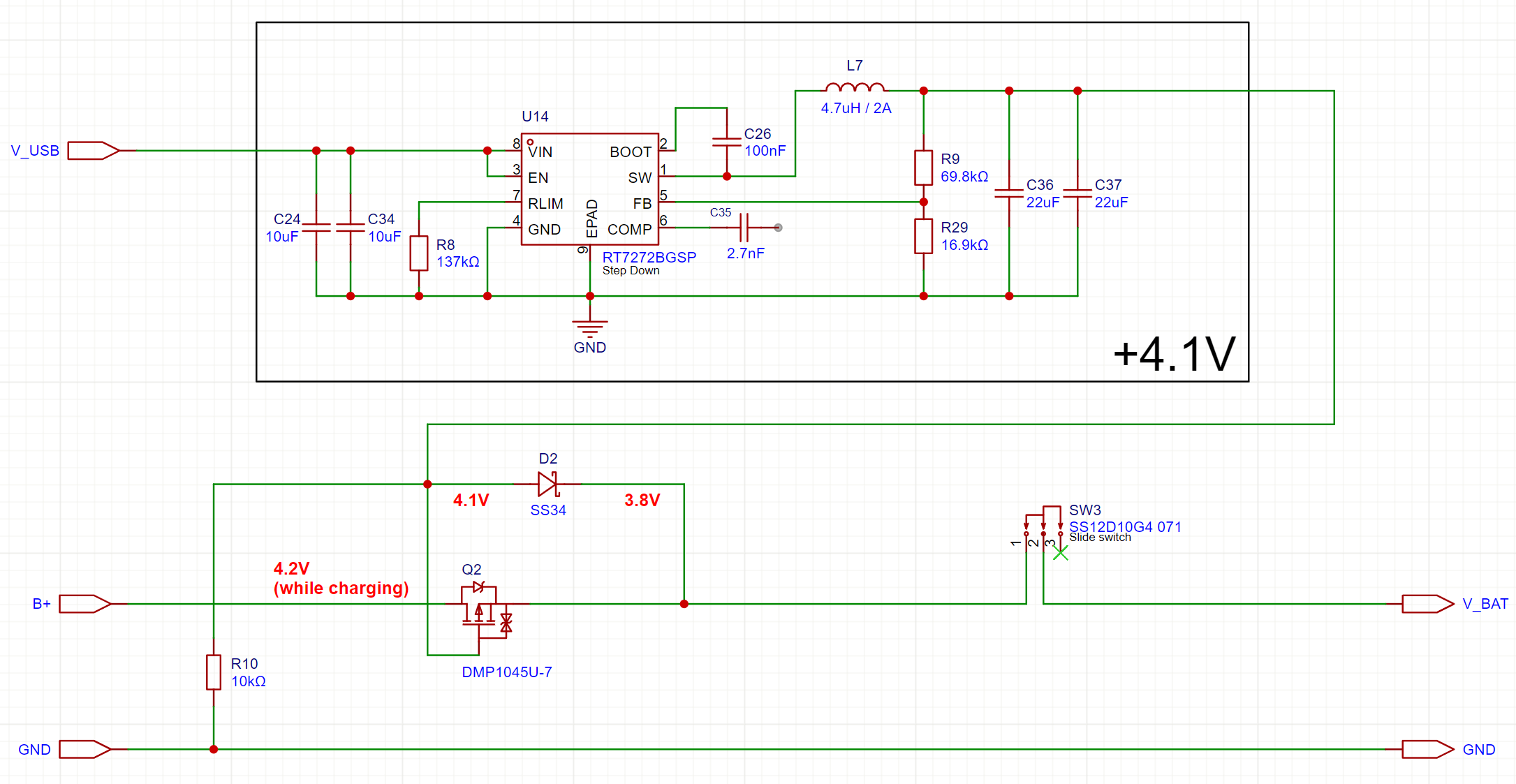
I've changed the power management circuit to the following.
Another problem occurs now: When not feeding in 5V as before, there might be current flowing through the body diode into the load circuit, which i do not want while USB is connected (the whole load sharing circuit is there to prevent exactly this).
See voltage markings below as reference.
Any idea how to solve this?
What do you think about this new schematic?
When a manufacturer specify something, they have taken into account margins. So that A7670 could probably be driven with 3.3 V too. Also, you got that C6 that should take care of power needs. If you're unsure that's enough, add another cap. Also make sure that C6 is as close the IC it can be, and then an optional cap.
No Nano symbol in your CAD? What program are you using? Not to criticize you nor the program, just curious.
I'm thinking that your charge IC could support both charging and the circuit, but you need an additional cap for those occasional power needs.
What's C5's task?
Edit: I stand corrected regarding C6 - from the datasheet: It is recommended to place four 33PF/10PF/0.1UF/1UF ceramic capacitors near Vbat to improve RF performance and system stability. At the same time, it is recommended that the Vbat layout routing width from the power supply on the PCB to the module be at least 2mm.
You need to redesign. In the example the 10pF is closest to the chip btw.
Yes, I think so. Or use the internal 8MHz oscillator. But I would like to see your buck converter output at 4.5V so it will be 4.2V after the shottky. There's no reason to make it lower than that.
I guess I've not been clear about that. You can't use the Nano pinout if you're using the PB chip. The Nano uses the P chip. They aren't the same chip, and don't have the same pinout.
No. The body diode is a regular silicon rectifier, and will need a 0.6V drop across it before current will flow. When USB is connected, the voltage after the shottky will be 3.8V as you've shown, or 4.2V as I recommended above, but in either case that's greater than the 3.6V the body diode would need before current will flow.
I've redesigned the circuit again. You gave me the confidence that it might work fine with 3.4V.
And i'd like to have a steady supply voltage for the ATmega328, because it will be driving LEDs and as far as i remember the output voltage is closely tied to the supply voltage, which would result in a different brightness of the LEDs, depending on the battery level.
I'm sorry i don't quite understand what you are asking here. I am using EasyEDAPro.
Good spot! It was meant to be between positive output and GND, not GND-GND
Are there any risks when using an external or internal 8MHz resonator? Most of the work of the ATmega will be sending text commands to the SIM module, and turning some LEDs/motors on.
Ok i've overseen that. I didn't order anything yet, so i think i will just go with the P version and use the Arduino schematics as reference.
The circuit is now the following.
If everything is fine with it, i will be adapting the ATmega to have 8MHz instead of 16MHz.
The only disadvantage of using a buck converter is that it needs the input voltage to be a bit higher than the output voltage you've set. I'm not familiar with the converter you're using, so I don't know how much higher than 3.4V the input needs to be. In fact, I've never found that spec in a buck converter's datasheet. Also, I don't know what actually happens when the input voltage is too low. Anyway, any required headroom has the effect of reducing battery life because the system shuts down at a higher battery voltage.
An alternative would be a buck/boost converter. It will work with input voltage above, below, or the same as the output voltage. But that's usually a more complicated circuit.
If you run directly from the battery, the system just runs until it doesn't work correctly anymore, which might be significantly lower than 3.4V, despite what the datasheets say.
I'm not going to be your best source on this question. I understand that the internal 8MHz processor may not be as accurate as a crystal would be, but I don't remember what the datasheet says about that. I think the OSCAL register can be used to calibrate the oscillator:
But otherwise I think the fuse settings have to agree with the type of crystal or resonator you're using if you go that way. But I've always just used a 3.3V 8MHz Pro Mini when I want to run an 8MHz Arduino. It has the 8MHz crystal already on it.
We haven't discussed how you are going to flash fuses and a bootloader to this chip, and how you will flash your sketch to it. Are you up to speed on all that? Do you have a programmer, or another Arduino you can use temporarily as a programmer? Do you have an FTDI UART adapter?
I guess you want the same pinout as in the IDE, otherwise you'd be using the ATmega328 symbol. But you're gonna have to to translate the Nanos pin numbering to the ATmega328s later on anyway... FYI.
I'm not planning to go below 3.5V anyway, because the LiPo doesn't really contain that much energy below that. I'd like to keep some safey margin (at least in the beginning).
I have adapted the schematics again. I replaced the 16Mhz crystal with an 8Mhz one, as well as the load capacitors (i'd like to use an external crystal and not the internal resonator). I also swapped the ATmega328PB chip for an ATmega328P-AU, as seen in the Arduino Nano schematics.
Also, there is this resistor which confuses me. Vcc and GND would be shorted like that?
Setting the fuse bits will be new for me. Seems like there are many tutorials online, but if you have a good and easy one which explains this, as well as burning the bootloader, i'm happy for recommendations!