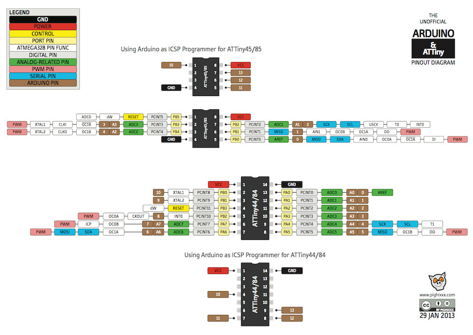
I am programming an ATtiny44 using Arduino as ISP Programmer under ATTinyCore. The PA0-PA7 works well as ouput lines with 0 to 7 respectively as their numerical addresses. For example: I can execute digitalWrite(7, HIGH) code.
Unfortunately, I cannot operate PB0, PB1, PB2 as output lines with 8, 9, 10 respectively as their numerical addresses. To activate these lines, I have to use bitSet(PORTB, PB0); and bitClear(PORTB, PB0) instructions instead of digitalWrite(DPin, HIGH/LOW).
Does anyone know the correct numerical addresses for PB0-PB3 lines? Or ATTinyCore has not defined their numerical addesses.
Say what? Pin mappings are arbitrary and can be different for the same chip in different "boards." If your board has board-level labels, you need to check which pin mapping is actually in use, assuming it's not some widely standardized board like an Uno or Nano. Any particular list of pin mappings cannot be "unacceptable", because it might be used on SOME board that SOMEONE sells.
In this case, there are two variants defined in ATTinyCore for the ATtinyx4, and they BOTH say PB3 is pin 11.
Also see the comment there: "PIN_Pxn notation is always recommended"
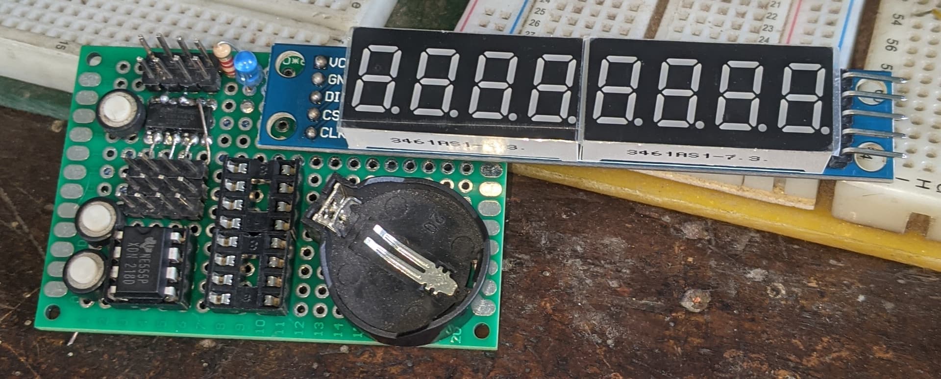
As I am using ATTinyCore for my ATtiny44 prototype board (Fig-1), I have understood that the pin mappings are defined there. So, regardless of Manufacturers variants, ATtiny44 should bear unique numerical addresses for the IO pins. For example:
Apparently I am not getting correct timing from TC1 of ATtiny44. Would appreciate to know the Fuse Bit values after performing "Burn Bootloader" process under ATTinyCore. This is to cross check the operating frequency of the MCU.
The fuse values depend on clocking and BOD levels, there are 15-20 options of fuse values just for a single Attiny44 chip.
See them in ATTinyCore/avr/boards.txt file. The description of Attiny44 chip with bootloader started from the 2818 line