amazed
January 29, 2022, 7:31pm
1
Hello, is it OK if VCC-AVCC pins are connected "below" the chip (highlighted trace)? (I'm not intended to use separate analog supply)
Another question is about the decoupling capacitors (C3-C4). Is it OK that they connect to ground through the pad of the uC? Or they need a separate via connection to the ground plane?
Thanks in advance.
LarryD
January 29, 2022, 8:11pm
2
Suggest you increase the width of the Vcc trace to 35-50mil.
Your Vcc trace between the two pads is okay.
The pin 1 on the capacitors should go to GND with a via just to the right of the pad.
Add ~100uF cap (as a reservoir capacitor) on your Vcc trace near the location where power is connected to the PCB.
amazed
January 30, 2022, 8:15am
3
Suggest you increase the width of the Vcc trace to 35-50mil.
This Vcc (branch) trace goes only to the uC. Wouldn't a 35mil trace unnecessarily wide for like max. 20mA?
The pin 1 on the capacitors should go to GND with a via just to the right of the pad.
Ok, thanks.
Add ~100uF cap (as a reservoir capacitor) on your Vcc trace near the location where power is connected to the PCB.
There is already a 10uF (value was suggested by the regulator datasheet) which is not shown on the clipping.
Paul_B
January 30, 2022, 11:50am
4
We are not talking about current.
We are talking about inductance .
amazed
January 31, 2022, 7:56am
5
Inductance comes into the picture if Vcc supply current has/could have high frequency components?
amazed
January 31, 2022, 11:28am
6
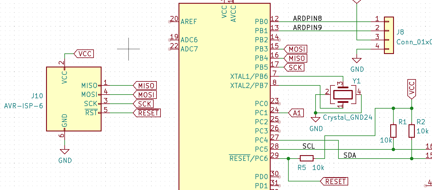
I'm trying to add a 6 pin ISP programming header also. It is just as the picture details, right?
MISO, MOSI, SCK are connected logically, ~RESET is connected in between the uC reset pin and the pull-up resistor?
srnet
January 31, 2022, 11:31am
7
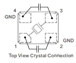
Your schematic says Y1 is a crystal, if so does it not need capacitors to GND on both sides ?
If you are using ADC of the MCU, then why not using LC filter for the AVcc supply to supress the switching ripples on the Vcc (digital) line?
amazed
January 31, 2022, 12:00pm
9
It is a 4 pin crystal resonator with built-in capacitors, only GND connection is needed if I got it rigtht from the datasheet .
@GolamMostafa : accuracy/noise is not that important for that one measurement. I used a Pro Mini board without problems before I started this separate PCB. (Pro Mini has VCC-AVCC directly connected)
According to the attached datasheet that is a crystal and it will need external capacitors. All my resonators are 3 pin devices.
amazed
January 31, 2022, 1:18pm
12
You are probably right. I add 22pF capacitors between 1-GND and 3-GND. Thanks for pointing it out.
amazed
January 31, 2022, 1:31pm
14
Yes, I mean 22pF between 1-GND and another 22pF between 3-GND.
amazed:
1-GND and 3-GND.
Mind that there two GND pads/pins; both have to used.
westfw
January 31, 2022, 9:08pm
16
I doubt it. They probably only connect to the case for shielding purposes...
Paul_B
January 31, 2022, 9:43pm
17
As suggested in the datasheet by "‧Extremely good for reducing EMI effect.".
I shot a series of videos designing a board based on the Nano. Take a look at these, they might help.
VIDEO
amazed
February 1, 2022, 8:54am
20
Thanks, pretty fresh stuff.
amazed
February 9, 2022, 10:36am
21
This will be a battery powered board and the time which the uC will be out of sleep is independent from the processing power, so I switched to 8 MHz to reduce current consumption. 8 MHz Crystal Resonator is a 2 pin component at the PCB prototype maker so I rearranged the layout (and also rotated the uC), this is what it looks like now: