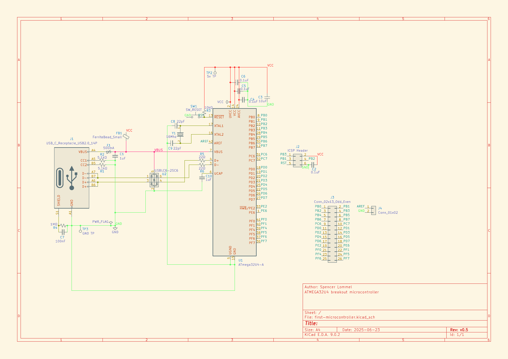
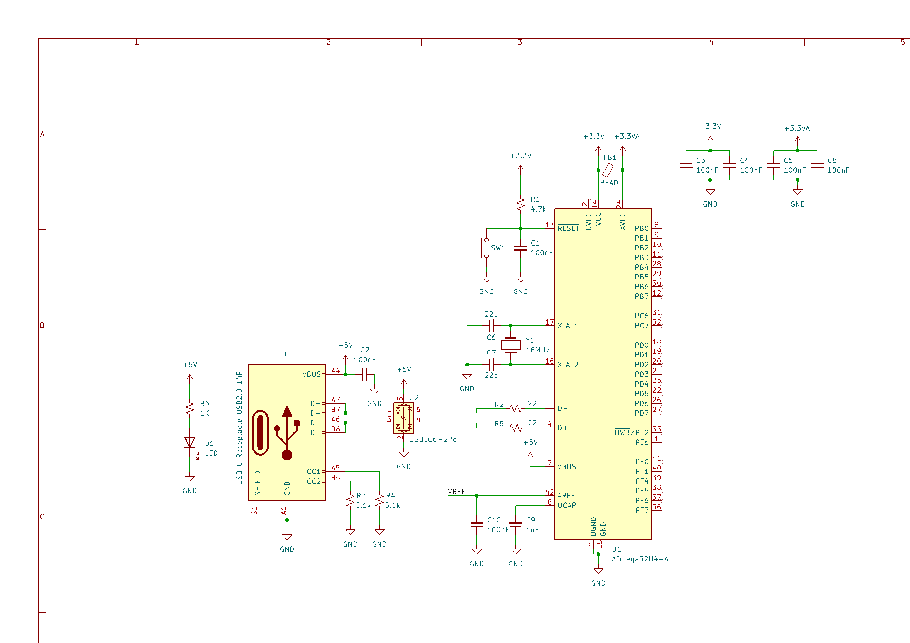
This is my first time doing PCB/schematic design with a microcontroller. I am making a development board based on the ATmega32U4.
I think my schematic is all correct and ready to start PCB design but I had a few questions if anyone could help out.
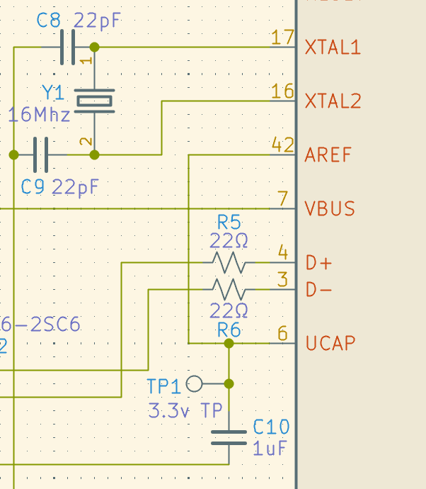
Is my oscillator (Y1) capacitor placement correct? and do these need to run to UGND like I have here?
I have a sort of separated 5v line. Before and after the ferrite bead. for any MCU related stuff I try and pull from the 5v after the ferrite bead is this correct?
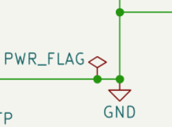
Should I have a separated GND for my MCU similar to how I have a separated 5v?
Is my 3.3v test pad (TP1) in the correct place?
If anyone notices any other issues with my schematic please let me know!
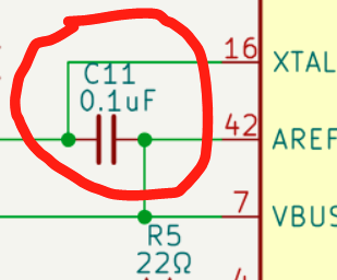
I did some research and it looks like you would usually connect AREF to an external 3.3v for analog reference. I don't think I'll use analog so should I just leave it like this?
Or is there a better solution where I can easily connect this? Would it be fine to route the 3.3v from UCAP up to this AREF or is that not stable enough?
I think Option 2 would be better I just don't know if this is supported or if I should connect somewhere else. The main goal of this board is just a simple board to teach myself schematic design so I don't really need analog features
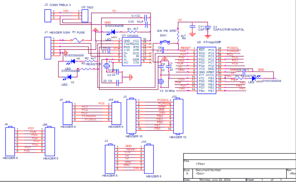
Before you make the PCB, prototype the system in veroboard and check that the system works to meet your requirements. See below my approach to build an ATmega328P Based (a colone of Arduino UNO) system: