Hello everyone,
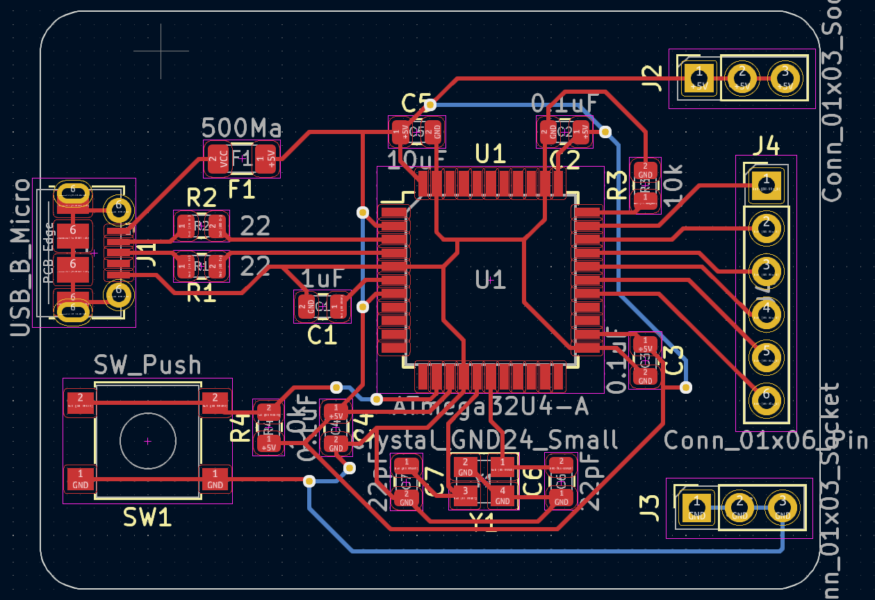
I just created a schematic and PCB for an ATmega34U4 using a guide and the documentation. I would greatly appreciate if someone could double check my work, as I am brand new to Kicad and this kind of project in general. I've uploaded my schematic and PCB layout, and also a zoomed view for clarity. I also have a GND fill zone that I omitted for clarity.
Thank you in advance!