I think I understand the CW vs CCW. In my words, since all functions are multiplexed to the pins, one can assume any internal path can be on any external pin.
My question is: Are the pins as shown in the Microchip ATTiny84(A) spec CW or CCW?
I'm also guessing the SCK MISO & MOSI are somehow defaulted to the pins shown in the above diagram, else how would you program the first program on a "blank" chip.
Not with an ATTiny84. (Assuming I understand the question. Which I certainly may not.)
In other words, physical pin 8, the one in the lower-right corner, is always MISO. MISO can never be a different physical pin.
...are one way to program the processor. Basically anything capable of controlling four digital I/O pins (RESET has to also be manipulated) can be used to program.
I believe dW (debugWIRE) can also be used but that requires a capable programmer.
I do not understand the clockwise / counter clockwise. If you're referring to pin numbering, it is always counter clockwise on any IC (or rather, I have never seen an IC where it did not apply).
I understand. But then how does this Clockwise vs Counter clockwise come into play? I would like to know which direction the identified pins (from their spec) are. I would really like to ignore this but it keeps coming up and I feel uncomfortable guessing or leaving the default and hope for the best.
I appreciate your help, as you might tell, I'm just starting with the ATTiny processors. And I have a character flaw, If I don't understand something, I'll likely never remember it.
It's just referring to how the physical pins are mapped to D0, D1, D2, etc identifiers. Originally ATTinyCore went counterclockwise, but switched to clockwise mapping later on.
From the pins_arduino.h files in variants/tinyX4_reverse and variants/tinyX4:
ATTinyCore old style counterclockwise pin numbering
Maybe your confusion is where to start counting. All ICs have an indication where pin 1 is.
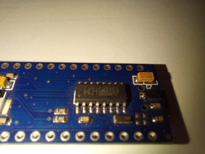
CH340; pin 1 is identified by the little dip (left bottom).
328P: pin 1 is identified by the little circle
328P: pin 1 is identified by the little dip (right bottom); note that the half moon matches the the top of your image (yes, I know it's a different chip).
Post #5 explains it all. The clockwise/counter clockwise option only refers to the Arduino numbering of the pins.
For example: The instruction
pinMode(7,OUPUT);
will refer to physical pin 6, ie register pin PA7,when using clockwise addressing. It will refer to physical pin 10, ie register pin PA3, when using counter clockwise addressing. Personally clockwise makes more sense to me.
However if you use the ATTinyCore recommended pin addressing the naming direction does not matter. Using PIN_PA7 will always refer to physical pin 6.
In a way this was the confusion, I've worked with 100's of IC's and every one was numbered CCW from the Pin #1 indicator, be it a dot or a angled corner or a 1/2 moon depression.