Can a certain 7-segment module work with Arduino IDE?

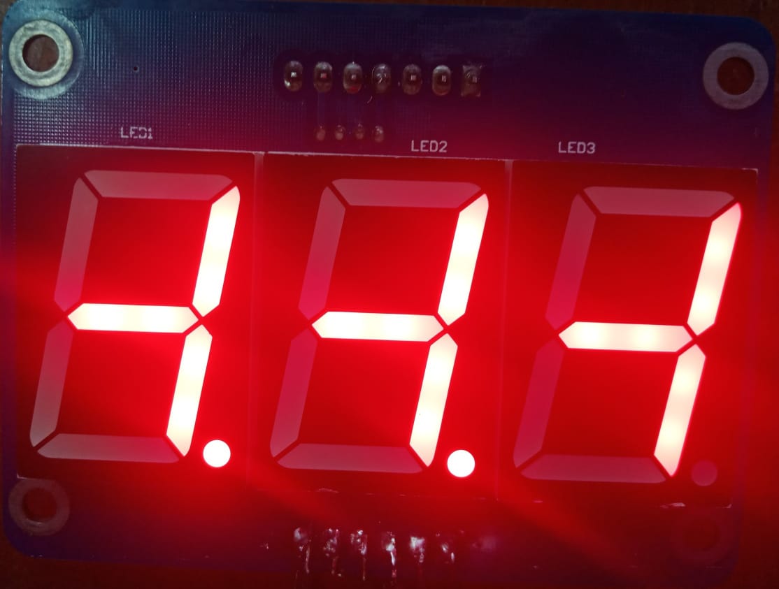
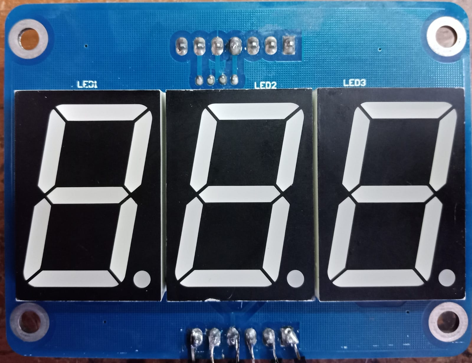
I have a 7-segment module like this:


The IC used here isn't 74HC595 (though CMIIW), and if I tried a code like this (which is used in some examples), only the 0 one worked properly, but not any of the other numbers (1-9):

#include "Wire.h"
#define LATCH 10
#define CLK 11
#define DATA 12

byte digit[10]= {0x3F, 0x06, 0x5B, 0x4F, 0x66, 0x6D, 0x7D, 0x7, 0x7F, 0x6F};
int i;

void setup(){
  pinMode(LATCH, OUTPUT);
  pinMode(CLK, OUTPUT);
  pinMode(DATA, OUTPUT);
}

void loop(){
  for(int i=0; i<10; i++){
    for(int j=0; j<10; j++){
      for(int k=0; k<10; k++){
      shiftOut(DATA, CLK, MSBFIRST, ~digit[k]);  // digit3
      shiftOut(DATA, CLK, MSBFIRST, ~digit[j]);   // digit2
      shiftOut(DATA, CLK, MSBFIRST, ~digit[i]);  // digit1
      digitalWrite(LATCH, HIGH);
      delay(50);
      }
    }
  }
}

Can these type of 7-segment module work with Arduino IDE? If it can, how to make the proper code in Arduino IDE that works with it?

OMG

:scream:

1 Like

LarryD is right. Also the soldering at the electrolytic capacitors is questionable.
The board is too old and too much damaged. Please don't use it.

1 Like

btw, TPIC6B595 is fine.it’s a high-current version of the 595 shift register family.

Just look,for 7-segment 595 shift register display…. after fixing the board.

1 Like

Try adding this before the first shiftOut() statement: digitalWrite(LATCH, LOW );
and increase the delay to 1000 ms.

1 Like

There is no line in your code to set LATCH to LOW, as @6v6gt said. These chips change their output when LATCH changes from LOW to HIGH, so that only happens one time when your code runs. That's why you see 0 but not 1 to 9.

This board looks like it may have almost caught fire once. That could happen again, so take great care with it.

1 Like

I've tried it, I guess still not working properly (for 1 to 9 part).

Did you see a well formed 0 (zero) on each of the 3 displays ?
Show the code that you used to make your latest test where you stated:

You can also remove this:

1 Like
#define LATCH 10
#define CLK 11
#define DATA 12

void setup() {
  pinMode(LATCH, OUTPUT);
  pinMode(CLK, OUTPUT);
  pinMode(DATA, OUTPUT);
}

void loop() {
  for (byte i = 0; i < 128; i++) {
    digitalWrite(LATCH, LOW);
    shiftOut(DATA, CLK, MSBFIRST, i);  // digit3
    shiftOut(DATA, CLK, MSBFIRST, i);   // digit2
    shiftOut(DATA, CLK, MSBFIRST, i);  // digit1
    digitalWrite(LATCH, HIGH);
    delay(1000);
  }
}

The results are like this:


That's what I meant for not working properly (for 1 to 9 part), there's well-formed 0 for 0 part, but the other numbers are like these.

Show the code which you used to generate this output.
If it is not displaying all zeros, is it always displaying exactly the figures shown in your image in post #10 or do you see random segments lit during the execution of the sketch ?

Did you repair the PCB?

1 Like

It looks to me as though we need to correctly identify which segment is controlled by which bit of the data that is sent to the TPIC6B595, and also whether the display is common anode, or common cathode.

Try this sketch, which should put on one segment at a time (same segment on each display), and note which order the segments are illuminated in.

#define LATCH 10
#define CLK 11
#define DATA 12

void setup() {
  pinMode(LATCH, OUTPUT);
  pinMode(CLK, OUTPUT);
  pinMode(DATA, OUTPUT);
}

void loop() {
  for (int i = 0; i < 8; i++) {
    digitalWrite(LATCH, LOW);
    shiftOut(DATA, CLK, MSBFIRST, 1 << i); // digit3
    shiftOut(DATA, CLK, MSBFIRST, 1 << i); // digit2
    shiftOut(DATA, CLK, MSBFIRST, 1 << i); // digit1
    digitalWrite(LATCH, HIGH);
    delay(1000);
  }
  // all segments off
  digitalWrite(LATCH, LOW);
  shiftOut(DATA, CLK, MSBFIRST, 0); // digit3
  shiftOut(DATA, CLK, MSBFIRST, 0); // digit2
  shiftOut(DATA, CLK, MSBFIRST, 0); // digit1
  digitalWrite(LATCH, HIGH);
  delay(3000);
}

Hopefully this will put on the segments in the following order: a, b, c, d, e, f, g, dp

7-segment-display

If not we will have a re-think.
(This is based on the assumption that they are common cathode 7 segment displays).

EDIT they will be common anode displays as PaulRB pointed out in post #15

I can't see how 0 can be well formed. The bit pattern for digit[0] contains 6x "1" bits, which would be correct to display "0", but the code inverts all the bits, which would cause only 2 segments to light.

They are driven by tpic6b595, so I think they will be common anode.

I hadn't spotted the "~" in the shiftOut() function.

(and I hadn't looked at theTPIC6B595 datasheet, to find out the outputs were open drain). So yes, the diplays should be common anode.

1 Like

Not necessarily but this is wild speculation until the OP comes back. There is a hex inverter on that board which appears to be connected to the 3 input lines SCL, LAT and DAT. The output of the gate connected to the DAT from the input connector block disappears into a via and may possibly also feed the first TPIC6B595 serial input. That is, an inversion may be done in hardware.
Having said that, the picture which the OP has shown in post #10 contains neither a valid character nor the inversion of a valid character so it is likely that the segment mapping table digit[] is anyway incorrect.

1 Like

that is why i provided sketch with sending simple numbers. most often blinking segment should be an "A"

I did not think of that!

I assumed the 74hc14 gates were connected in pairs and used as buffers. Yes, it's possible the data line is inverted. But... why do that? After all, writing a 1 to the output of a tpic6b595 connected to a common anode display lights the corresponding segment. An obvious and intuitive way to design the circuit. Why ruin that by inverting the data? Perhaps we will never know.

I'm using this one:

#define LATCH 10
#define CLK 11
#define DATA 12

void setup() {
  pinMode(LATCH, OUTPUT);
  pinMode(CLK, OUTPUT);
  pinMode(DATA, OUTPUT);
}

void loop() {
  for (byte i = 0; i < 128; i++) {
    digitalWrite(LATCH, LOW);
    shiftOut(DATA, CLK, MSBFIRST, i);  // digit3
    shiftOut(DATA, CLK, MSBFIRST, i);   // digit2
    shiftOut(DATA, CLK, MSBFIRST, i);  // digit1
    digitalWrite(LATCH, HIGH);
    delay(1000);
  }
}