@Wawa Thanks a lot for this information, I google it and it is very helpful! Very good materials about it on this forum as well, thanks!
I finish the V1 of the schematics and PCB, taking into account everyone's contribution, for you guys to have a look. Feel free to comment! Thansk for sharing all this knowledge.
@jim-p@Wawa - As I'm getting more and more into this circuit, I'm learning a lot. By looking at your reference for "power supply decoupling", I understood it's function - 1) to drive momentary power to the IC if needed, 2) to filter undesirable frequencies in the circuit.
2 questions - You mention that Tiny 10uF tend to fail faster - this applies to tantalum? Any reason to use it or not to use it? Same is valid for SMD ceramic?
Second, in one of the searches, i found - "Still other rules-of-thumb require decoupling capacitors spread evenly over every square inch of the board. - The EMC problem requires that a distributed capacitor strategy be used. That is, the capacitors should be distributed over the entire board. This is not inconsistent with the functionality requirement, since a capacitor near an IC can serve both purposes easily.
It has also been shown that the actual value of the capacitor is not important. It is recommended that the largest value of capacitance within the selected surface mount package size be used."
So should I place a few caps around the board ( it has 18,5cm by 7,5cm)?
Should I increase the value of the caps near the ICs (standard is 1uf on designs) to 100uf with no problem in performance?
First of all, I want to say THANK YOU for sharing this video. Amazing information. I watched a few times and it's really good, highly recommend for other people to watch. With that, I went into another sprint to learn more, and I decided to restart again from scratch ;).
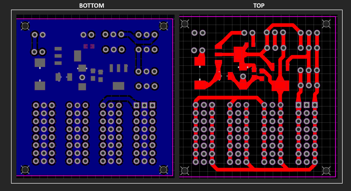
With that in mind, I started to redesign the power supply, trying to calculate the Di/Dt, understand more about the components, and not using autorouter.
So here is the layout for the "power supply" part, that I would love to hear your opinion. Consider this a practical use in a simpler circuit, to see if the concepts I learned aligned. Also, because I saw that power supplies generate noise, so they will be more controlled if tied togheter in specific areas of the board.
I enlarged the Vias, holes and paths, to match the di/dt (in theory) lol.
Added the power led, reviewed all connections.
I would really appreciate your help understanding:
Design is good (or better)? Any considerations?
My choice of components ( I decided to reevaluate based on my calcs and select each component as I learn) is good?
Overall thoughts
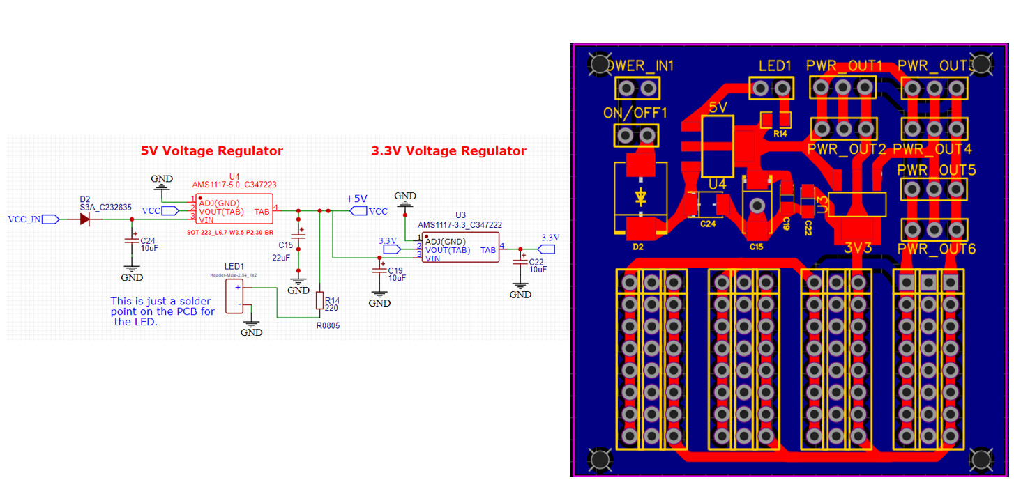
For this "breakout" the concept is a board being powered from 7-12V, and supplying the pins with 5V or 3.3V 800mA (ams1117) . 5V takes the input voltage, and from the output drives the 3.3V. Here is the schematics, and a back and front view of the board. The pins have 3 rows (5V/GND/3.3) and 6 "independent" power out for other breakouts... just a concept.
There is no need to for 45° corners for traces, analysis and testing has proven this is not needed except in extremely, extremely high frequencies which we will never be involved with.