Hi Guys,
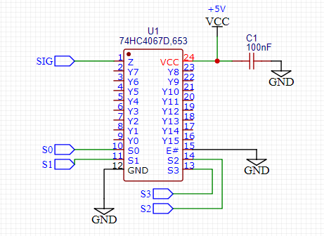
I'm trying to convert a project I have into a full PCB with no extra modules. I'm using 8 of those cd74hc4067, and I want a more expert opinion if the main wiring for this is correct:
Hi jim-p, thanks for the quick answer! No, I will not have this situation. They will be used mainly for reading buttons, faders etc. I don't plan on chaining them as well, since the code will get more complicated.
Hi sorry for the delay, I was updating the schematics. It's not yet a finished version, but you can have an idea. It's like a breakout board with mux for Analog / digital, later I'm adding 12C and Led matrix, with Midi In/Out ports. So it can be used for controllers as well.
Thanks LarryD. I will work a little more on the project and repost. I have to change the 74HC4067D,653 for the 74HC4067DB,118 due to availability. Will be back in a few hours or a day! Thanks for the insights.
Seems a lot easier to just use the modules pictured in post#1, with a 16-way ribbon cable soldered to each module, and then stack them with 2-3mm spacers on the mounting holes.
Bare wires straight through all the pins on the other side, connecting VCC/GND/S0-3/etc.
Leo..
Thanks Wawa. I already have a solution like this, where you can plug the leonardo and the modules. what I'm looking for is a way to have more ready and less solder , integrated pcbs, also to reduce size.. and maybe a little of challenge and fun along the way lol.
JLCPCB will manufacturer your board even if your violate their minimum requirement, but don't expect it to work.
Their min annular ring for a PTH is 12 mils. You have a via dia of 24 with a drill of 12, that gives an annular ring of only 6 mils ((24-12)/2). Their capabilities table is confusing with many contradictions.
I would use the following:
Drill = 20 mils
Via = 48 mils (annular ring = 14)
Trace = 15 mils minimum. Make power and ground as big as possible
Clearance = 15 mils minimum.
Don't tent the vias, they can be valuable test points when debugging.
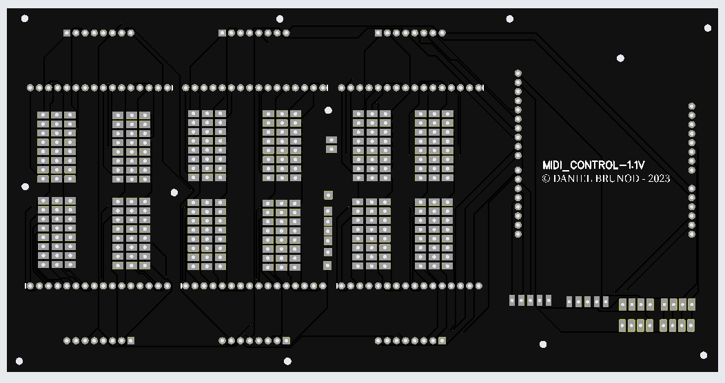
So i've made a few changes, trying to acommodate the suggested parameters for the board. I had to tweak a little due to the SMD components, but it's looking better. I've also made a bottom GND copper layer, and a top VCC (5V) top layer. Added a TCA9548A for multiplexing 12C ( enabling up to 8 devices, same address ex. oleds) . Componentes were mounted to one side only, for cheaper and easier assembly. Still need to add a Midi in and out and a led driver for led inputs and outputs + power on. Let me know your thoughts!
Quick Question(s) - I'm adding a MAX7219 to drive leds, so when buttons or controls are pressed, the can be used for a panel. I have found 3 different schematics:
MAX 7219 being driven by a 74HCT125 - as I understand, it's used as a signal buffer - Necessary?
Matrixed LED displays can add noise to the power supply rail, that needs to be suppressed.
Google "power supply decoupling".
It is common to have a ceramic cap and an electrolytic cap in parallel. They both cover (kill) a different frequency spectrum. I would have used 47 or 100uF instead of 10uF. Tiny 10uF electrolytic caps tend to dry out (fail) faster.
Leo..