Hi guys, I just designed a SPDT pin but I don't understand it, is the picture correct?

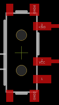
Your diagram appears to show a switch that can connect the VCC pin to 3.3 V
Is that what you want to do ?
Yes, that's right. I still don't understand about the smd switch.
The SMD switch footprint shows 3 connections to its contacts but you cannot tell from the footprint which pad is connected to which contact internally
It would be conventional to have the centre pad, ie pad 2, as the common connection and for the other pads to be the NO and NC connections of the switch but it is impossible to tell from the diagram or image of the footprint whether this is the case
Do you have the actual switch available to test its connections ?
What is the switch part number?
Yes I have it but I still don't understand because the datasheet doesn't explain the pin names based on the leg location.
If you have the switch then you can use a multimeter to figure out which pad is which
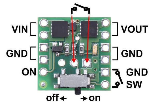
This MSK12C02
It's on the last page of the datasheet
Or click on the CAD model link
Does that mean I only need a ground line at number 4?
Only if you want the metal casing connected to ground but it's not necessary for switch operation
So is my pin writing correct?
Do you want the case connected to ground?
No need, I just need to turn off the supply like in the 2 pin spst switch
I connected it with esp32 3v
Your footprint does not match the one in the data sheet. The pin numbers are reversed and it looks like some of the pads are larger.
To be sure everything is right I would find the correct footprint for that switch.
Also if you show the pin numbers on your schematic, it would be clear as to what is connected to what.
Ok if you can tell me just tell me which pins i need to change i just want to connect from battery to switch then go to esp 3v pin
You can connect Vcc to pin 2 and 3.3V to 1 or 3 and ignore the other pads.
However, I would make sure that is the correct footprint for that switch and not wait till you get the PCB and find it does not fit.
I saw someone made it like this using pin 1 for the ground path, I'm not sure
But there are also those who explain it this way

I just need clarification on which one is correct