Body to follow. Just to see if I can post
In early development work on a project, I place components on a standard punchdown board and add flying leads as needed. If I need a little more durability, I’ve gone to using stripboard(link below), which has a 27X35 grid of solder holes, with rows interconnected by continuous copper strips. I temporarily place my devices on the stripboard, make strip cuts to interrupt current flow as needed, then add in soldered wires to interconnect the strip segments to finish the circuits.
I wanted a design tool to aid in this process, and I used the macro language embedded in Microsoft Excel for that. Picture 1 shows the first sheet of the macro-enabled Excel tool, for a project having an ESP32 S3 DevKitC-1, two BigTree Trinamic 2209 driver boards for stepper motors, a BROK buck converter, and a small I2C display showing the IP address of the user interface for the project.
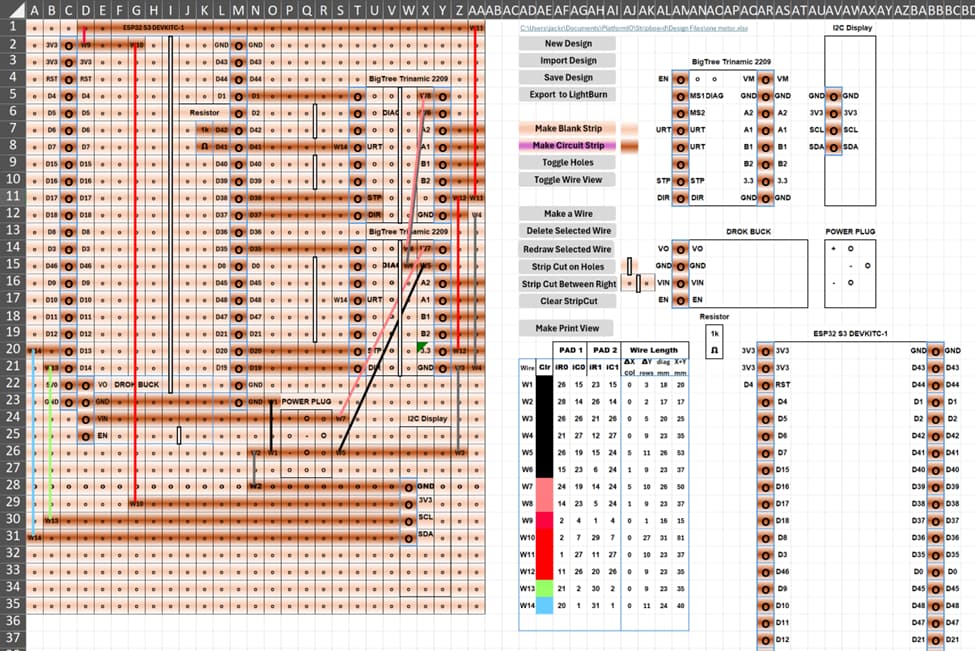
The left section of the pic shows the layout of the stripboard, with portions of the strips that are part of a circuit in the darker color. Strip cuts either over or between holes are shown, as are the colored interconnect wires.
The mostly grey boxes to the right of the design area serve as command links to various macros. The top four (New, Import, Save and Export) are file commands. The middle four boxes are for maintenance of the design area visuals. The next six command boxes are associated with wire making and strip cutting. The bottom Make Print View command first creates a top and bottom view of the design area on a separate Excel sheet, then formats and prints the pair in landscape mode, handy for use during actual soldering.
Below the commands, a table of wires showing wire color, starting and ending solder pads, and the length of wires (mm) needed for the connections, calculated for two different routings. Clicking on any of the colored boxes brings up a dialog to change the wire color.
The other items on the right side of the pic are taken from other sheets in the Excel file, which have additional information (pinout diagrams, pin usage guides, Amazon order links, pin assignments, personal notes etc.).
I’ll be posting another topic on how to easily make strip cuts using an electric Wen carbide engraver ($12 on Amazon), with guides I designed and 3d printed.
Anyone interested in trying out the tool should Private Message me.
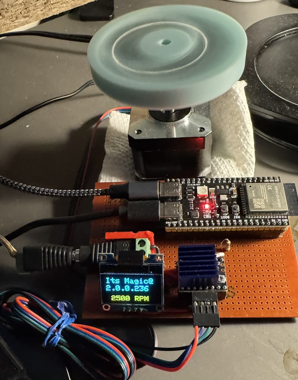
Finally, here’s a picture of a version of the design I made with only one BigTree, with the NEMA 17 stepper running at 2500 RPM, as shown on the display. I think it can go faster, but I chickened out because of worry about the flywheel structural integrity.
Stripboard: Amazon.com
1 Like
Nice. I don't use Excel but I'm sure some people would like to use it. Can you post the sheet / macros?
I use KiCad, set the grid to 0.1”, and tell it I’m using a 2 layer PCB. Then I use the bottom copper layer for the strips, marking cuts with an X. For wire links I use the top copper layer.
1 Like
Nice but looks like a lot of work to create the Excell sheet.
I just print even spaced dot in Excell and print it and draw what I want to build.

1 Like
Kicad has already been suggested and this method looks quite impressive: Perfboard circuit design with Kicad
If you have a license for Microsoft Office, you have Excel and the underlying macro language called Visual Basic for Applications. It’s under the Development tab that must me enabled in Excel, I believe. It’s a full object-oriented language with a wonderful IDE and debugger. This forum will not allow direct uploading of a macro-enabled Excel file. I do have a website where I have a section for such material for downloading, and I’ll work to get that going in the next few days. In the meantime, if anyone knows how to do this more expeditiously, let me know.
Also note that, while I did this for stripboard PCBs, it works just fine for any other type of solder board having 0. 1” hole spacing. You just need to add more wires for a given project. The project I posted had some 27 connections needed, and the strips took care of all but 14 of these. That was important to me because I’m 81 years old, have severe arthritis in the hands, and failing eyesight. My solder station has a video microscope projecting to a 4K TV for solder joint inspection! Not great solder joints as you can see, but good enough for hobby work.

Stripboard can be challenging to get clean joints due to the way the solder likes to wick down the tracks. There is a type of stripboard that has solder mask over the tracks, providing the type of "pads" we are accustomed to soldering on standard PCBs. I find this type of stripboard to be much more pleasant to work with:
I purchased mine from AliExpress. I don't generally recommend AliExpress since I have had bad experiences (I stopped using it some time after I purchased a stock of stripboard). I would guess you can find the same product on alternative marketplaces like eBay and Amazon.
2 Likes
That is the problem ![]()
Long ago, while still working, I did use that at occasion.
Thanks for the great tip. I found the item below on Amazon that appears to be the same thing with a solder mask. Arrives Thursday and I’ll give it a try. …
1 Like
I've developed my own prototype strip board, partially inspired by an Adafruit design. The tracks are easy to cut, where not required, and solder does not flow across the strip.
Rear side. No solder mask except around the perimeter:

Front side. The solder mask is actually white and the silk screen markings in black. On this side, there are no copper tracks between the pads. The lines shown between the pads are only silkscreen markings:

.
1 Like
Very nice! I think the plated through holes are an important advancement over the standard stripboard (including the type I use with the solder mask).