First an apology. I accidentally reposted this post. I do understand the time and effort put in by people who reply to posts, and it was not my intention to demand their time by repeating the question. I really appreciate the ideas that come forward. It was an accident. Yesterday I was under advice from a doctor not to undertake anything "critical". It seems I should have taken that advice more seriously, since I made a mistake I would not normally. Today I was discharged by the same doctor as able to return to normal duties. Sorry again for my mistake, and I will try to be more careful.
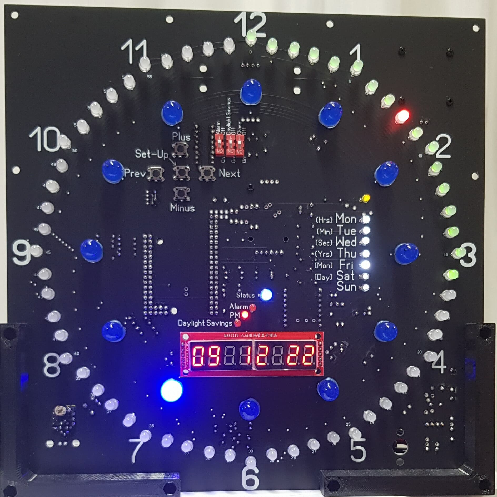
Secondly, I draw attention to the project which this query is part of. It is an "analogue" LED clock, pictured showing the date and time at: 07:08:16 PM on Friday 9 December 2022.
Clocks like this are not really new, this is just my take on it. In this instance, I have installed the eBay "red" pre-built module for this picture. The project is clearly working, if still in development. I want to make two points: 1) the PCB for the 7 segment LED module is nothing like as complex as the whole working clock PCB. 2) I am not phased by debugging a PCB. The first version of the clock board didn't work as intended, but after some debugging work, I was able to locate and fix the errors. I certainly don't have the hubris to believe that my PCB's never contain errors. The bi-colour outside LEDs are "Charlie-plexed" and I am really happy with the result.
So a number of questions and assertions have been made:
> You missed a real test. You're still assuming that the problem is not on your board.
I may appear that I have assumed that my PCB is bullet proof, but I have made tests I have not listed - as it was my post was too long (as is this one). So my position is currently that it is possible the PCB has errors, but on balance, I consider that to be the lower probability, until other evidence emerges.
> Part swapping:
That is an excellent plan. I already swapped the 7 segment LED modules with known good ones to no effect. I have ordered some MAX7219 IC's from a known good source and await their arrival with baited breath and depleted bank account.
> You have to accept the fact that your continuity checking may not have been complete.
I completely agree that continuity checks are limited in scope. In addition to basic point to point "expected continuity", I have also checked that points which should not be joined are, in fact, not. The latter takes much longer than the former. So effectively I have checked that everything that should be there, is there, and that anything that should not be there is not there. (The latter is an illogical test and always flawed, but I have done what I can - It is like asking everyone who can't hear me to put their hands up). For all that, points which should be connected are connected, points which should be isolated are isolated.
> IC closeup photo:
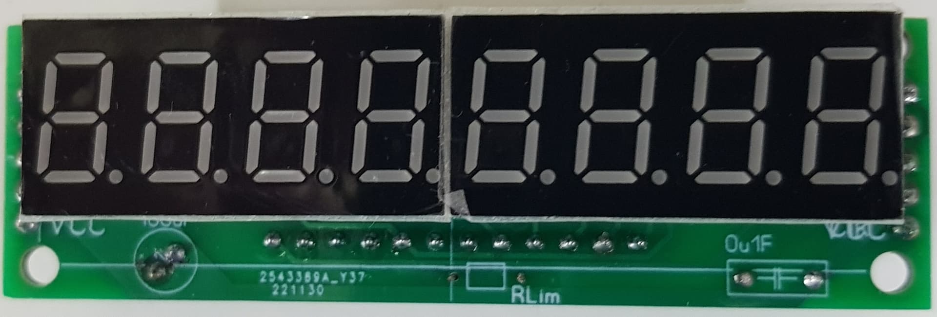
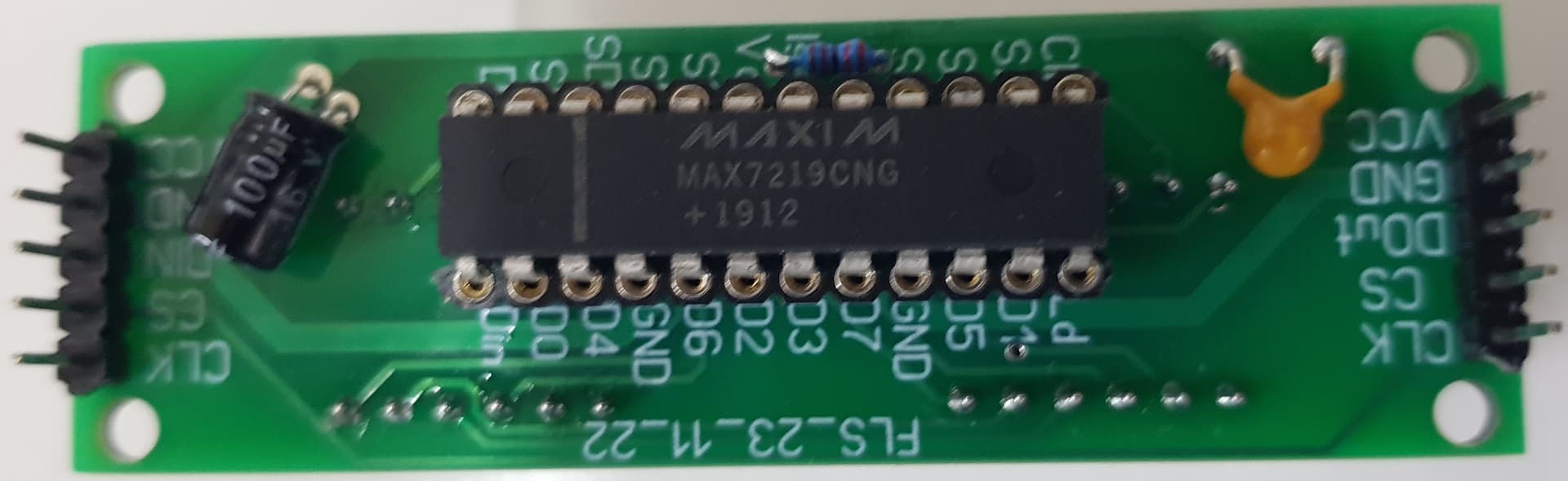
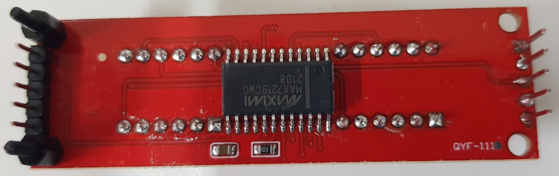
See photos attached of my green board. These MAX7219 share some identifiers to cloned devices, and all devices I have are marked the same. But at least they spell MAXIM correctly, unlike on the red eBay board.
If you need better photos still, I will do my best.
> How did you design the circuit?:
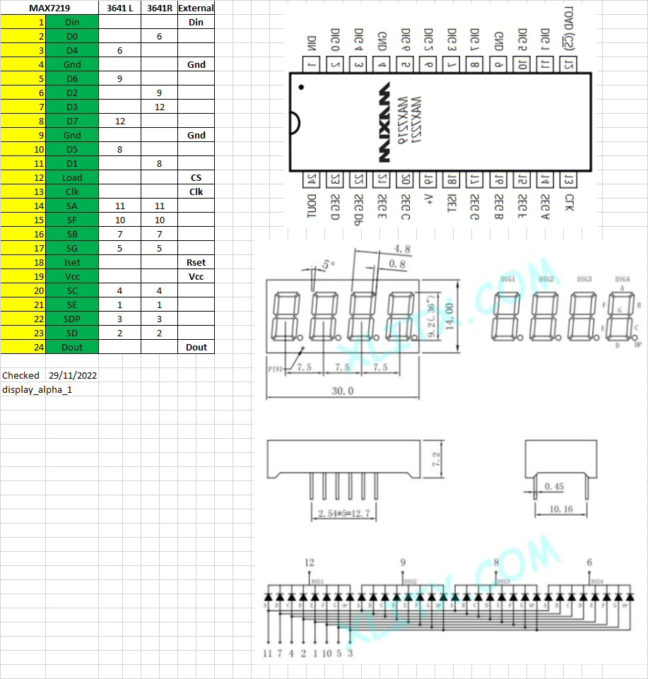
I design all my circuits with reference to manufacturer data sheets. The data sheet I used has the reference number 19-4452; Rev 4; 7/03 at the top left of the first page and is attached for perusal. I did not draw a formal circuit as I am basically using the same one as in the data sheet in the drawing "Typical application circuit" bottom right of the first page. Instead of a formal circuit I used a pin interconnection map. This map is included as the image pin_connections.jpg. My board has the same pinout to the external circuit as the red eBay board, so I could interchange them. As good practice, bypass capacitors are included on the board. Before you tell me I have transposed the connections to the MAX7219 remember it is mounted on the back of the board.
max7219_datasheet.pdf (712.7 KB)
Also, there is an unrelated error on this board, no prizes for spotting it, but I will be interested if anyone sees it.
> How many PCBs do you have?:
- At this point I have only built one as they only arrived a couple of days ago and since my close encounter of the medical kind soaked up most of yesterday and a good chunk of this morning, I have not had a chance to build another. Good idea though.
> Continuity checks are ok, but if the trace is too narrow it won't carry sufficient current:
That's true enough. To help stop such errors creeping in, I run with design rules enabled on all of my board designs and have the design software check for a range of potential rule violations on a regular basis as I lay the board out, and certainly before I get any made. Things like narrow traces, traces too close, overlapping holes, et al. This board complies with the design rules easily, the minimum track size on the board being 0.4mm.
As to the current drawn by the display, see page 11, Table 11, of the MAX7219 data sheet which covers off the selection of RSet which fixes ISeg. The LEDs are red, so I would expect VLED to be about 1.8 volts or so I chose a 22K resistor which gives an ISeg in the high 20's mA, depending how you read that table and how much that table applies to cloned chips. Say 30mA worst case for a segment.
A bit too high still, perhaps, but OK for a test. The red eBay board uses 10K for red LEDs!!! Yikes.
That gives a total figure of 30mA * 8 = 240mA down the throat of the MAX7219 digit driver, and associated track, if a digit has all the segments and the DP lit. A short 0.4mm track will cope with that, possibly with some voltage drop, but not enough to fuse the track or kill the LED output completely. I always use the largest trace I can, but in this case I was running traces between IC pins and 0.4 mm seemed a reasonable compromise between track width and track spacing.
PCB layout is attached as a zip file containing the Gerbers and the drill file. I didn't know how else to post this. It is visible with any Gerber viewer. I use Sprint Layout for my PCBs.
display_alpha_1.zip (15.5 KB)
Here some experiments with series resistors in the SPI lines worked:
I had not seen this before and will try it out. This looks like a timing or signal echo scenario with damping resistors fitted to minimise the problem. In any case, it is easy enough to experiment with.
> You can make these devices a bit more predictable if you have an external pullup resistor on the Load/CS pin to prevent it floating at system start.
Agreed. I normally include this on the "mother board", in this case the black LED clock board and a check verifies I have fogotten. So much for bullet proof boards.
Finally, I have also posted some images of the eBay board, red in colour. Both back and front shots are shown. For reference only. Notice MAXIM is spelt MAXIMI.
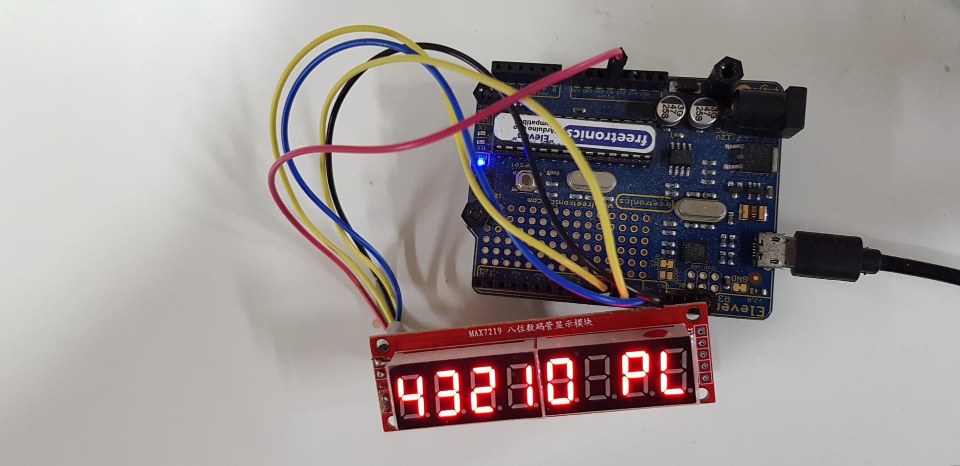
Here is a shot of my test jig with a working red eBay board under test:
Thanks for suggestions. Regards,