Hallo Leute, ich möchte dieses Jahr etwas tiefer in die Programmierung der STM32 Mikroprozessoren einsteigen.
Ich habe mir dazu ein Arduino Portenta h7 board zugelegt und bin nicht zufrieden was die Programmierung an geht.
Da mein Augenmerk immer auf die ADC und DAC Komponenten fällt, habe ich zerst den DAC getestet:
#define SAMPLING_RATE 2000000  // Sampling rate (Hz)
#define AMPLITUDE 32767       // Amplitude of the sinusoid (16-bit)
//#define PI 3.14159265358979323846
#define FREQUENCY 1000000  // Frequency (Hz)
#define F_CPU_ACTUAL 480000000

static inline void delayNanoseconds(uint32_t) __attribute__((always_inline, unused));
// Wait for a number of nanoseconds.  During this time, interrupts remain
// active, but the rest of your program becomes effectively stalled.
static inline void delayNanoseconds(uint32_t nsec) {
  uint32_t begin = DWT->CYCCNT;
  uint32_t cycles = ((F_CPU_ACTUAL >> 16) * nsec) / (1000000000UL >> 16);
  while (DWT->CYCCNT - begin < cycles)
    ;  //wait
}

void setup() {
  CoreDebug->DEMCR |= CoreDebug_DEMCR_TRCENA_Msk;
  DWT->LAR = 0xC5ACCE55;
  DWT->CYCCNT = 0;
  DWT->CTRL |= DWT_CTRL_CYCCNTENA_Msk;
  // Set the PA4 pin as an output
  analogWriteResolution(16);
}

void loop() {
  // Generate the sinusoid
  unsigned long beginT = 0;
  for (int i = 0; i < SAMPLING_RATE; i++) {

    int16_t value = AMPLITUDE * (sin(2 * PI * i * FREQUENCY / SAMPLING_RATE));
    analogWrite(A6, value + AMPLITUDE);

  }
}
Ich habe in diesem Beispiel mit Absicht eine hohe Abtastrate gewählt und auch mit Absicht delayNanoseconds nicht in der for schleife aufgerufen.
Die Maximal ausgegeben Frequenz ist gerade mal 32kHz. Das ist nix. Weshalb ist das so langsam??
Laut appNode, kann der DAc weitaus mehr als 1Mhz, wenn man die entsprechenden Register aktiviert.
Habe dann mal nachgesehen wie analogWrite aufgerufen wird:
Ok, es wird also ein Umweg über mbed OS gemacht und die Werte in Prozente umgerechnet.
Das ist natürlich ein quatsch.
In der AnalogOut.h findet man eine write_u16 Funktion
Da dachte ich dann ok, schriebst alt in der wiring_analog.cpp Datei eine neue Funktion:
"analogWrite_u16(...,...)" (der Rest sollte jedem klar sein )
Geht aber nicht, weil die arduino ide diese Funktion nicht finden kann.
Miene frage an euch: Weshalb wird meine neue funktion nicht gefunden. ich kann keine Header Datei finden wo man eine neue Funktion eintragen muss.
Ich habe mir dann auch noch mbed OS Studio heruntergeladen. Wenn ich mir dann die Fabrizierte bin Datei in den Flash-Speicher schreibe (unter beachten des bootloaders), leucht die grübe onboard LED nur noch dauerhaft.
Also hier komme ich auch nicht weiter. Ich möchte ungern den Bootloader löschen.
Zufrieden wäre ich wenn man direkten Register zugrif via der stm32h7xx_hal.h Dateien haben könnte oder direkt mbed OS Style programmieren könnte.
wenn es eine .cpp gibt muss es auch eine zugehörige .h geben. Nur habe ich vom Portenta System keine Ahnung. Wenn du aber lieber direkt programmieren möchtest, dann lass setup und loop weg. Programmiere einfach klassisch mit main ohne Arduino Framework. Andererseits hättest du das Geld für Portena nicht ausgeben müssen. Ein Teensy oder ein STM32 Nucleo hätte es auch getan.
Stimmt, an die STM32 Nucleo Boards habe ich gar nicht gedacht^^
Die Teensy nutzen einen NXP Mikrocontroller und diese sind aufgrund des Chipmangels kaum zu bekommen. (Bis auf Teensy 4.x)
Einfach so auf höhere ebene Programmieren geht leider nicht. Es fehlen die Reverenzen zu den Hardware abstraction layer Dateien (HAL Dateien).
Aber, es gibt tatsächlich eine Header Datei wo analogWrite vor kommt:
Man kann aber mbed os Style programmieren:
#include "mbed.h"

#define SAMPLING_RATE 2000000  // Sampling rate (Hz)
#define AMPLITUDE 32767       // Amplitude of the sinusoid
//#define PI 3.14159265358979323846
#define FREQUENCY 1000000  // Frequency of the sinusoid (Hz)
mbed::AnalogOut* dac1 = NULL;

int main() {
  dac1 = new mbed::AnalogOut(digitalPinToPinName(A6));
    while (1) {
        unsigned long beginT = 0;
        for (int i = 0; i < SAMPLING_RATE; i++) {
            beginT = micros();
            int16_t wave = AMPLITUDE * sin(2 * PI * i * FREQUENCY / SAMPLING_RATE);
            dac1->write_u16((uint16_t)wave);
             unsigned long endT = micros()-beginT;
            wait_ns(1.0/SAMPLING_RATE*1000*1000*1000);
        }
    }
}
Aber jetzt mit write_u16 sehe ich kein Sinus mehr sondern eine Dreieck Wellenform.
Ab einer gewissen Geschwindigkeit kommt nur noch eine "verrauschte" Gleichsspannung.
In den Datenblättern steht was von einem internen Operationsverstärker, diesen muss man abschalten. Aber wie? Ohne die HAL Dateien keinen zugriff auf die Peripherie.
ich denke auch eine HAL muss es geben in den Tiefen der Ordnerstruktur. Arduino kann ja nicht zaubern. Such mal nach stm32h7xx-hal. Für sich gesehen findet man es auch hier. https://github.com/stm32-rs/stm32h7xx-hal
Ansonsten bist du vielleicht hier besser aufgehoben. Portenta H7 Forum
Ja, die HAL Dateien gibt es.
Aber ich muss zu jeder Datei einzeln die absoluten pfad angeben.
Dann hast du in den header Dateien selbst wider Pfade zu header Dateien, die dann auch nicht mehr stimmen. Das ist alles ein Krampf.
Ich habe auch schon versucht code via STM32CubeIDE zu kompilieren, aber ist ist auch das gleiche Problem. Einige HAL Dateien sind nicht bekannt und wenn ich den Pfad absolut angebe, kennt es die Klassen nicht usw. .
Ich bin davon ausgegangen das sich das Portenta Board wie ein Teensy programmieren lässt.
Weshalb der in mbed OS Studio kompilierte code nicht startet, habe ich auch noch nicht begriffen. ich glaube das hängt mit dieser libmbed.a Datei zusammen.
Ich habe schon versucht einen compilierten code vom stm32 core auf den Flash zu laden.
Dann leuchte die grüne led auch nur dauerhaft.
und zwar wenn hier hdac.Instance = DAC; statt hdac.Instance = DAC1; steht kompiliert er nicht
Weil, DAC schon als Pin Makro hinterlegt ist
Ich habe dann einfach via undef das Makro gelöscht, was allen Anschein nach alle DAC Makros in den Hal Dateien löscht und dann geht nix mehr.
So compiliert der code erst ein mal. Aber es passiert nix am DAC pin. Wascheinlich wird der dac im mbed core schon anderweitig initiiert.
– 12-bit left alignment:  [15:4] bits
– 12-bit right alignment: [11:0] bits
Die Zahlen in den eckigen Klammern sind die Bitpositionen nach Wertigkeit. 2 hoch n.
Das wird vermutlich ein 16Bit Register sein, dann stehen die 12Bits je nach Konfig am linken oder rechten "Anschlag".
probiere erstmal mit niedriger Frequenz bspw. 100Hz.
Die 1MHz vom DAC werden sich auch kaum auf eine Sinusausgabe beziehen.
Berechne mal wieviel Zeit deine Berechnungen für eine Schwingung benötigt.
Du hast 360 Stützwerte. Jede Stützwertberechnung benötigt Zeit.
1MHz hat eine Periodendauer von 1 µs.
Eine Berechnung dürfte demnach nur 1/360 µs dauern.
Oder anders gesagt eine Schwingung muss in unter 1µs durch sein.
Ist das möglich? Prüfe das.
Wenn das zu lange dauert musst du die Werte vorberechnen und in einer Tabelle ablegen. Das geht in Richtung DDS.
Davon abgesehen ist noch offen ob der DAC überhaupt hinterherkommt. Schau nach welche "Updaterate" der DAC hat und berechne mittels Anzahl der Stützwerte was überhaupt theoretisch machbar ist.
Ja, ist ein 16 bit breites Register aber weshalb kann man dann nur 12 bit Werte hinein schreiben?
Bzw was ist der Hintergedanke für diese Art der Register?
Am DDS bin gerade dran, scheiter aber noch am DMA Transfer. Bzw leuchtet die Orangefarbene LED des Totes.
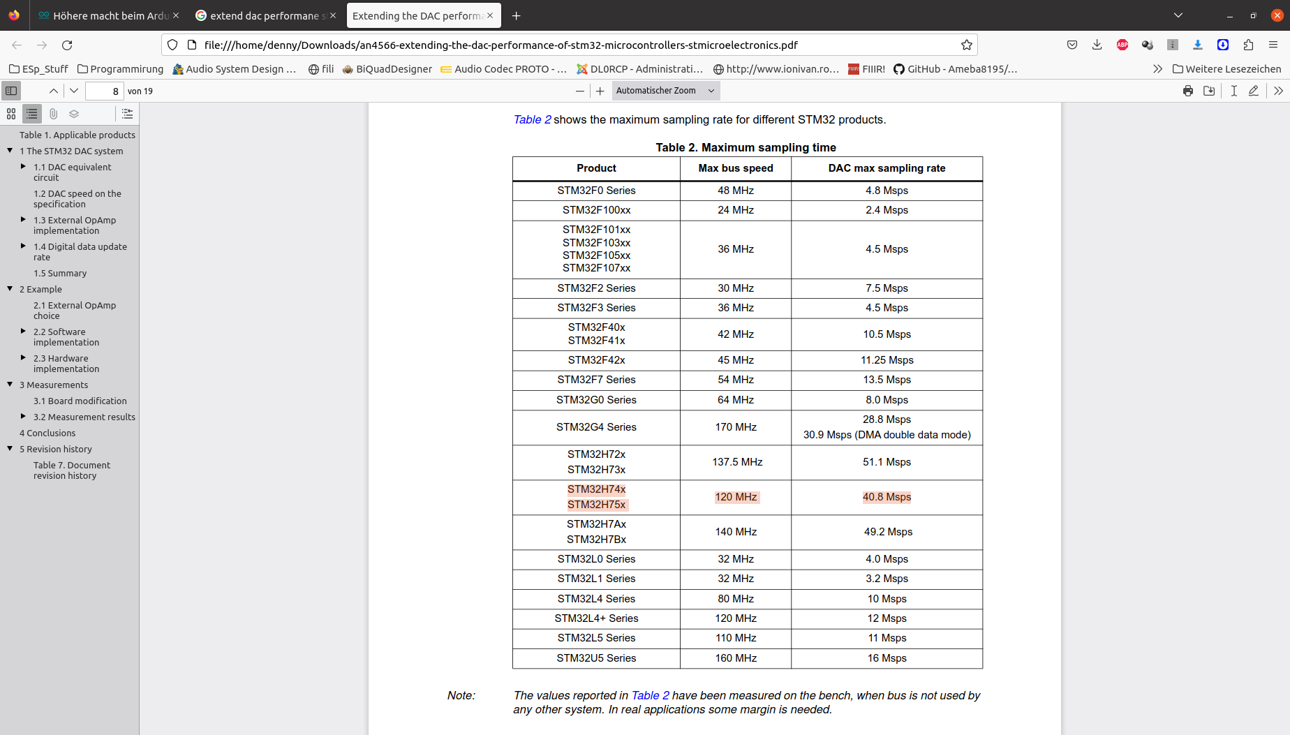
Hm laut AN4566, geht der DAC bis 40.8 Msps. Das sollte für 1Mhz sinus genügen.
1.4 Digital data update rate
The STM32 DAC output data need to be written to the DAC holding register (DHR), then the
data is moved to the DAC output register (DOR) for the conversion.
Generally, the data are saved in a RAM, and the CPU is in charge of the transferring the
data from RAM to DAC.
When using the DMA, the overall performance of the system is increased by freeing up the
core: data go from memory to DAC by DMA, without need for any actions by the CPU. This
keeps CPU resources free for other operations.
The trigger of the DAC conversion can be done by the software, external triggers, or by the
timers. For the high speed conversion cases, it is recommended to use the timer trigger in
combination with the data transfer done by the DMA.
The transfer speed from memory to the DAC is limited by several factors, among them:
the clock cycle of the APB or of the AHB (DAC clock)
the DMA transfer cycle from memory to the DAC (includes the AHB to APB bridge)
the trigger mechanism itself.
The DAC on STM32F407x microcontrollers is running on the APB1:
three cycles after the trigger, DHR data is moved to the DOR register
at the same time a DMA request is generated from DAC to DMA
DMA transfer takes at least one APB clock cycle.
So a total of four APB clock cycles is needed to update the DOR data. As APB1 maximum
clock is 42 MHz (for ST32F407x), 10.5 Msps is the maximum update rate for the DAC
output register when timer trigger and the DMA are used for the data update.
The minimum transfer clock cycle by DMA to the DAC is not the same for all STM32
microcontrollers, because of the different bus configuration
Ich habe noch nicht richtig begriffen was APB und AHB für Register sind.
...aber langsam, sind ja nur ~3000 Zeilen Datenblatt
Ja, das ist mir schon klar. Aber wozu 12 bit in einem 16 bit Register? Man hätte ja auch ein 12 bit Register nehmen können und nicht so ein voodoo mit "left alignment" und "right alignment "betrieben müssen.
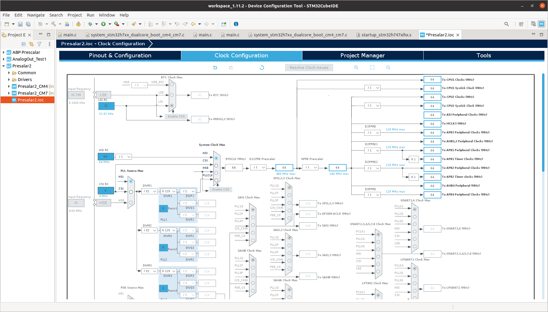
Bei dem "APB Gedöns", habe ich jetzt im Datenblatt RM0399 eruiert, dass der DAC vom APB1 clock Register angetrieben wird. Seite 496 Absatz 9.7.44.
Demzufolge muss der Prescaler vom APB1 angepasst werden.
Siehe Schema:
Unter Punkt 9.7.8 findet man dann die Register für den Prescaler.
Demzufolge müsste der Befehl "RCC->D2CFGR = RCC_D2CFGR_D2PPRE1_DIV16;". die DAC Ausführung verlangsamen, aber es tut sich nichts.
K.A was nun das Problem ist.
Ja, macht Sinn^^. Haben die wahrscheinlich konstruktionsbedingt so gemacht.
Ich habe jetzt mal andere Messmethoden und Debugging Methoden aufgezogen.
Ich habe diesen Sinus berechnung's Quark weggelassen und stattdessen. in einer schleife die Spannung "langsam" erhöht und auch reduziert.
#include "stm32h7xx_hal.h"
#include "stm32h7xx_hal_rcc.h"

#define F_CPU_ACTUAL 480000000

static inline void delayNanoseconds(uint32_t) __attribute__((always_inline, unused));

DAC_HandleTypeDef hdac1;
HAL_DAC_StateTypeDef dacState;


void initDAC1() {
  DAC_ChannelConfTypeDef sConfig = { 0 };
  // Enable clock for DAC
  __HAL_RCC_DAC12_CLK_ENABLE();


  // Initialize DAC
  hdac1.Instance = DAC1;
  hdac1.State = HAL_DAC_STATE_RESET;
  if (HAL_DAC_Init(&hdac1) != HAL_OK) {
    // Initialization Error
  }

  // Disable output buffer
  //hdac1.Instance->MCR &= ~(DAC_MCR_MODE1_1 | DAC_MCR_MODE1_0);


  sConfig.DAC_Trigger = DAC_TRIGGER_NONE;
  sConfig.DAC_OutputBuffer = DAC_OUTPUTBUFFER_DISABLE;

  if (HAL_DAC_ConfigChannel(&hdac1, &sConfig, DAC_CHANNEL_1) != HAL_OK) {
  }

  HAL_DAC_Start(&hdac1, DAC_CHANNEL_1);
}


void initRCC_DAC1() {
  RCC->D2CFGR = 0;
  RCC->D2CFGR |= RCC_D2CFGR_D2PPRE1_DIV1;
}

// Wait for a number of nanoseconds.  During this time, interrupts remain
// active, but the rest of your program becomes effectively stalled.
static inline void delayNanoseconds(uint32_t nsec) {
  uint32_t begin = DWT->CYCCNT;
  uint32_t cycles = ((F_CPU_ACTUAL >> 16) * nsec) / (1000000000UL >> 16);
  while (DWT->CYCCNT - begin < cycles)
    ;  //wait
}

void wait_DAC1() {
  do {
    dacState = HAL_DAC_GetState(&hdac1);
  } while (dacState != HAL_DAC_STATE_READY);
}


void setup() {
  HAL_Init();
  CoreDebug->DEMCR |= CoreDebug_DEMCR_TRCENA_Msk;
  DWT->LAR = 0xC5ACCE55;
  DWT->CYCCNT = 0;
  DWT->CTRL |= DWT_CTRL_CYCCNTENA_Msk;
  Serial.begin(9600);
  initDAC1();
  initRCC_DAC1();
}

void loop() {
  uint16_t out = 0;
  uint16_t out_2 = 4095;
  unsigned long beginT = micros();
  for (uint16_t i = 0; i < 4095 * 2; i += 5) {
    if (out < 4095) {
      HAL_DAC_SetValue(&hdac1, DAC_CHANNEL_1, DAC_ALIGN_12B_R, out);
      out += 5;
    } else {
      HAL_DAC_SetValue(&hdac1, DAC_CHANNEL_1, DAC_ALIGN_12B_R, out_2);
      out_2 -= 5;
    }
    wait_DAC1();
  }
  unsigned long endT = micros() - beginT;
  Serial.println(endT);
}
Man kann die Taktung auch via HAL libaray einstellen:
Weshalb die ausgegebene Frequenz nun Schneller ist, aber der Schleifen Durchlauf insgesamt langsamer verstehe ich noch nicht.
Vermutlich Prüft HAL_DAC_SetValue ob der DAC bereit ist, wenn nicht überspringt er die Funktion. Damit wäre mein Aufruf von wait_DAC1(); überflüssig.
Nebenbei ist das Portenta H7 nur mit 400Mhz getaktet:
4kHz sind jetzt auch nicht unbedingt das was ich erwartet habe.
du hast den Prescaler vom DAC geändert? Warum?
Um die Frequenz des Dreiecks zu beeinflussen musst du die Ausgabezeitpunkte an den DAC beeinflussen können. Nicht den DAC selbst. Der DAC muss nur nachkommen was er scheinbar tut. Du willst letztlich die Periodendauer ändern zusammengesetzt aus deinen Stützwerten.
Stell dir eine Tabelle mit DAC Stützwerten vor die dem DAC kontinuierlich übergeben geben. Je schneller die Werte immer nacheinander an den DAC übergeben werden desto größer ist die Frequenz die mit dem DAC erzeugt wird. Dazu wird nicht der DAC geändert sondern die Pausen zwischen den Wertübergaben an den DAC. Der DAC muss nur schnell genug sein um nichts zu verzögern, der muss quasi immer bereit sein sofort einen neuen Wert entgegen zu nehmen. Prüfen kann man das dennoch, darf aber nicht stören. Ansonsten wäre man schneller wie der DAC zulässt.
Letzten Endes wirst du um die Verwendung eines Timers nicht drumherum kommen.
Hallo Doc_Arduino
Es geht mir primär erst ein Mal darum heraus zu finden wo die Grenzen des DAC's liegen.
Es steht ja geschrieben, das man mit den Software Timer bis 555kHz ausgeben kann. Aber ich komme nicht auf solche Frequenzen.(und vorallem 555kHz von was?? ein/aus oder Sinus...) Mit DMA sollen dann noch höhere Ausgabe Frequenzen möglich sein. Aber DMA steht auf einen andern Blatt. ich will erst mal das Software setting durch probieren.
Jedenfalls meine wait_DAC1 Funktion ist Schmutz. HAL_DAC_STATE_READY prüft nur ob der DAC bereit ist zu wandeln nach der Initialisierung, nicht aber ob eine Wandlung statt findet.
Ob eine Wandlung statt findet, diese Flag scheint es gar nicht zu geben.
Es steht nur:
Bit 15 BWST1: DAC channel1 busy writing sample time flag This bit is systematically set just after Sample and hold mode enable and is set each time the software writes the register DAC_SHSR1, It is cleared by hardware when the write operation of DAC_SHSR1 is complete. (It takes about 3 LSI periods of synchronization). 0:There is no write operation of DAC_SHSR1 ongoing: DAC_SHSR1 can be written 1:There is a write operation of DAC_SHSR1 ongoing: DAC_SHSR1 cannot be written
Aber das ist für den Sample&Hold Modus.
Wie bekomme ich den nun heraus das eine Wandlung statt findet? Mann könnte ja zur Not noch die Takte zählen die der DAC benötigt für die Wandlung, aber selbst das finde ich nirgends geschrieben.
Jedenfalls:
Ohne meine Misslungene Wait Funktionn komme ich auf 44kHz. Die Prozessor Taktung habe ich auch entsprechend auf 480Mhz angepasst. (Eher copy / pasted^^).
Aber Achtung die Arduino Entwickler haben nicht umsonst den Takt auf 400MHz hinab gesetzt.
Es ist so, das der MC34PF1550A0EP Spannungsregler nur 3,1 statt 3,3 Volt ausgibt.
Übertaktet man den STM32H747, bricht irgendwan die Spannung ein und dann ist Schluss.
Da habe ich doch gerade was gefunden. RM0399 Seite 1094: If the software trigger is selected, the conversion starts once the SWTRIG bit is set. SWTRIG is reset by hardware once the DAC_DORx register has been loaded with the DAC_DHRx register contents.
Aber heute nicht mehr, geh jetzt zum Sport und dann ist der Tag rum.
Ja also, ich bin jetzt mit meinem Latein am ende. Den software Trigger für den DAC, den habe ich ja überhaupt nicht aktiviert. ich habe ja Trigger none:
sConfig.DAC_Trigger = DAC_TRIGGER_NONE;
Geschrieben steht dazu:
Das bedeutet also sobald ich etwas in DHR12R1 schreibe, wird es ausgegeben.
Es ist auch ziemlich komisch beschrieben im Datenblatt: Depending on the loaded DAC_DHRyyyx register, the data written by the user is shifted and stored into the corresponding DHRx (data holding registerx, which are internal non-memory- mapped registers). The DHRx register is then loaded into the DORx register either automatically, by software trigger or by an external event trigger.
Weiter unten dann: Data stored in the DAC_DHRx register are automatically transferred to the DAC_DORx register after one dac_pclk clock cycle, if no hardware trigger is selected (TENx bit in DAC_CR register is reset). However, when a hardware trigger is selected (TENx bit in DAC_CR register is set) and a trigger occurs, the transfer is performed three dac_pclk clock cycles after the trigger signal.
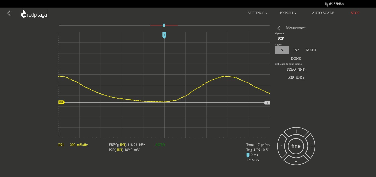
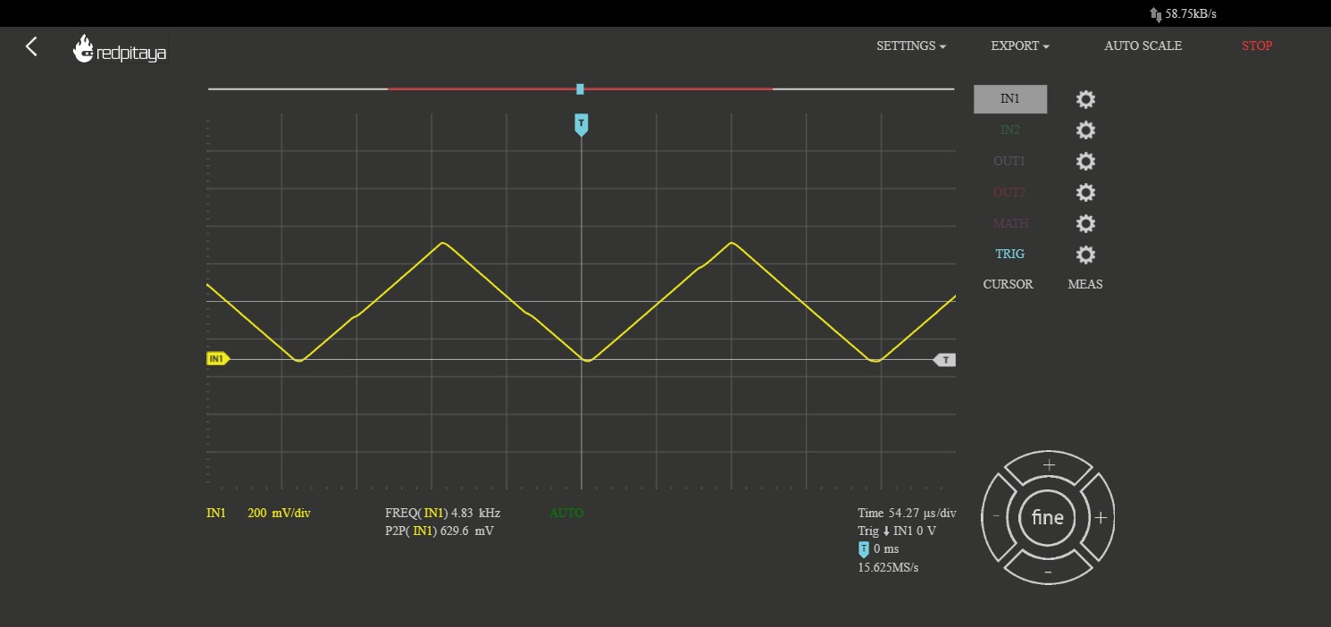
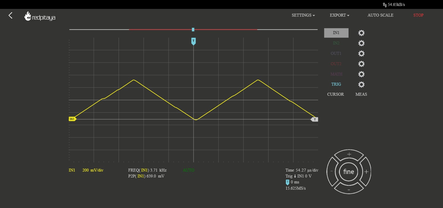
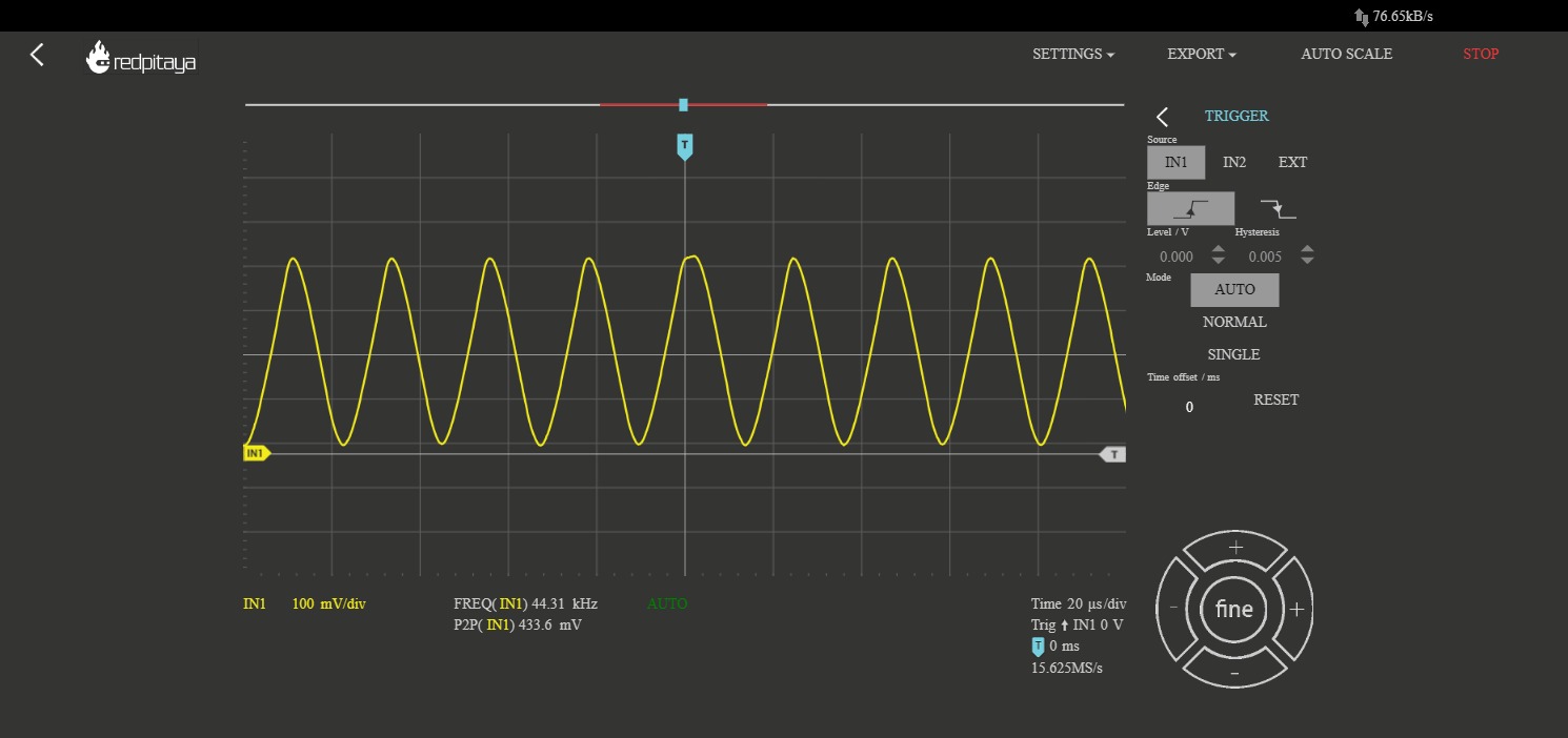
Ohne irgendeine "Warte Funktion" sehe ich auf meinem red pitaya, was ich als Oszilloskop benutze eine 44kHz sinus:
Ich vermute, das die DAC Ausgabe so schnell von statten geht, das das red pitaya gar nicht richtig schnallt, das ich nur die Spannung von 0 auf 4095 Digital Werte erhöhe und von 4095 auf 0 absenke in 480Mhz Geschwindigkeit.
Jedenfalls lass ich den Beitrag ab hier edieren. Dafür, das ich zuvor noch nie mit dem STM32 gearbeitet habe, bin ich schon gut vorwärts gekommen.
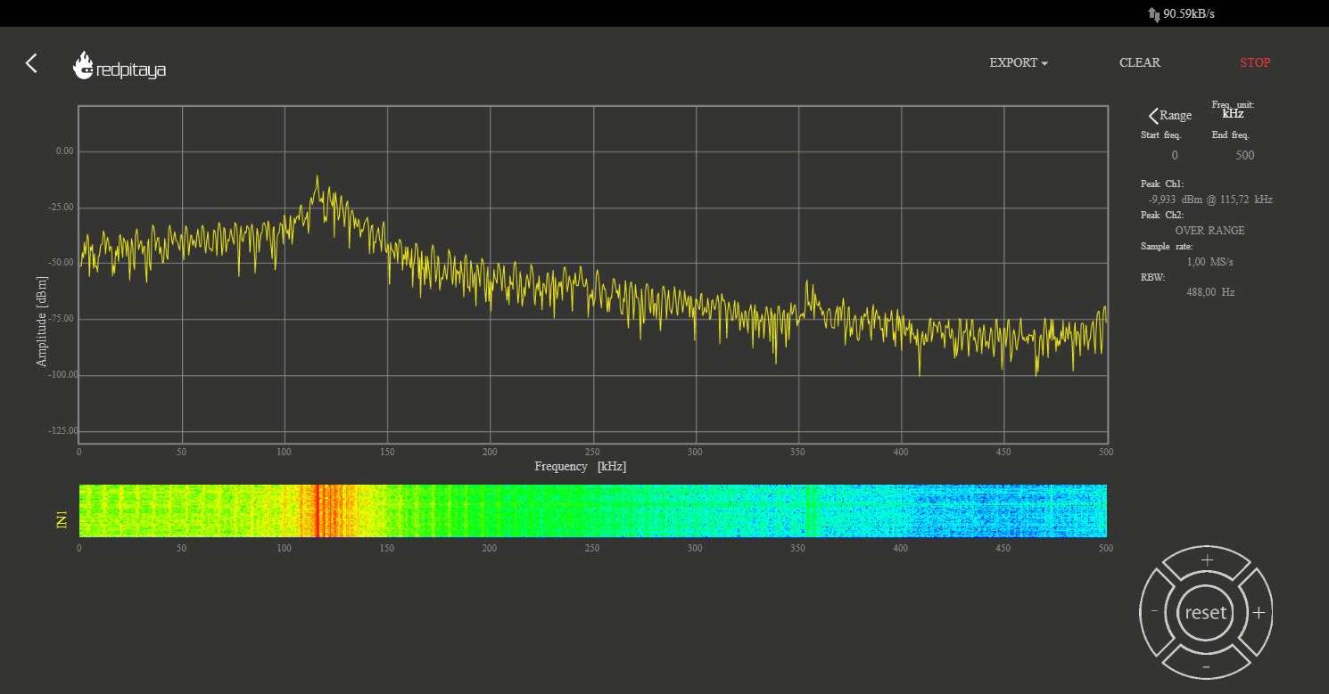
du musst dir schon vorher im Klaren sein was geht und was nicht. Du wirst sicherlich einen red pitaya mit 125 Msps haben. Damit kann man maximal Frequenzen mit dem halben Wert abtasten, also max. 62,5MHz. Ganz grob um überhaupt eine Signalform zu erkennen. Stichwort Abtasttheorem.
Außerdem wie schon einmal gesagt, dein Sinus kann niemals 480MHz betragen. Mach dir doch einmal den Ablauf der Signalerzeugung klar. Ich weiß nicht was der Controller so kann. Aber nehmen wir einmal an der DAC könnte einen Wert jede ns ausgeben. Dann kannst du ein Rechtecksignal mit Periodendauer von 2ns. erzeugen. Willst du dagegen ein Sinus mit 360 Stützwert ausgeben dann reden wir schon von einer Periodendauer von 360ns. Und weil der DAC sicherlich nicht im ns Intervall arbeitet ist das entsprechend langsamer. Rechne die Periodendauer in eine Frequenz um. Male dir den Ablauf auf und führe dir es vor Augen. Zur Controllerprogrammierung kann ich dir sowieso nicht helfen. Dafür gibts das passende Unterforum.