NOW I ADDED A MAKEFILE TO FLASH DIRECT WITH AVRDUDE THE AVRGCC C90 PROGRAM Added -D in flash. IS BELLOW. I REVISED AGAIN Missing * for pointer value. CHANGED DELAY MICRO BY UTIL/DELAY.H _delay_us(). I ADDED FRITZING CIRCUIT AND THREE OPTIONS OF CONTROLLER IN THE CODE. I am trying to use and LCD 16 x 2 and shows only black boxes with a library example and with a direct port manipulation program that I want to implement. Controller HD44780 don't mention in the datasheet a command to determine internal pullups BIAS resistors FOR WAVE VOLTAGE IN FRAME 1/16. But ST7070 yes. I have no experience in it at all. I want to know if this can be the problem and which pullups are convenient because I use only 4 data and other are not connected and can send bad values without a resistors.
Command in St7070 rs:0 rw:0 D: 000001xx in the datasheet xx 2.2k, 6.8k and 9 k
CAN BE THIS THE PROBLEM ?
THIS IS THE CIRCUIT DRAWING:
https://drive.google.com/file/d/105jxT2YLWTsHt7iJGs_oO9WbeYaBA4UH/view?usp=drivesdk
Photos are these:
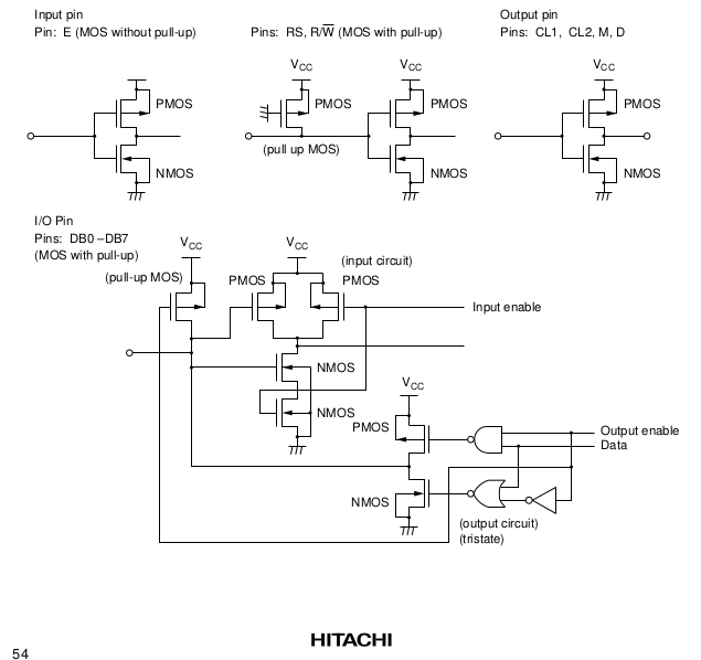
This is the datasheet print screen with the set extended functions mentioned in ST 7070
https://drive.google.com/file/d/1EQPdluNiqCxRsXbA6WAnaVhnrrmUHsPe/view?usp=drivesdk
https://drive.google.com/file/d/1EPQ_VJhpxoP5XvzmEixg1-sP0pPcM3zq/view?usp=drivesdk
https://drive.google.com/file/d/1EQaa9kTp2FsJuegxwTxgaiT7awEoMsvJ/view?usp=drivesdk
https://drive.google.com/file/d/1EUGiz4xFTWN6ae5Oteb8voL4pkIm3WbV/view?usp=drivesdk
The unfinished code is this:
#include <avr/io.h>
#include <avr/interrupt.h>
#include <util/delay.h>

#define F_CPU 16000000UL

// I gonna use a delay making a watchdog and interruption to permit other operations
// during display startup
// THIS IS FOR WATCH DOG PRESCALLER TIMER WHILE A DELAY IS RUNNING OTHER OPERATIONS
// CAN BE DONE UNTIL LCD FINISH ITS DUTIES
// WATCH DOG CLOCK IS 128 KHZ 7.8 MICROSECONDS
// THE REGISTER OF WATCHDOG IS WDTCSR
// FIST 4 BITS DETERMINE THE TIMEOUT LIMIT BY OVERFLOW
// 0000 (WPD3, WPD2, WPD1, WPD0) LIMIT IS 16 ms
// 0001 is 32ms
// 0010 is 64ms
// 0011 is 125 ms
// 0100 is 250 ms
// 0101 is 0.5 s
// 0110 is 1 s
// 0111 is 2 s
// 1000 is 4 s
// 1001 is 8 s
// rest are reserved bits
// WDTCSR |= 1 <<< WDIE6 ENABLE WATCHDOG INTERRUPT (BIT 6)


// THIS IS LCD HANDLING USING DIRECT MANIPULATION
// AND AN LCD LCM 1602 A WITH ST7063 CONTROLLER
// IMPORTANT NOTE LCM1602A AND ST7063 AND HD 44780 ARE DIFFERENT I WILL LEAVE INITALIZATION FUNCTION FOR THE THREE TYPES
// ENABLE TIME FOR INITIALIZATION IS NOT DEFINED IN DATASHEETS THAT IS SOMETHING AMBIGUOUS ASSEMBLY EXAMPLE DONT USE ANY
// DELAY BUT IS MANDATORY A DELAY IN READ AND WRITE THAT PULSE REQUIREMENTS VARY FORM 400 TO 1200 nS
// DARIO LOBOS 13/MAY/2025


// THESE ARE BITWISE FUNCTION NEEDED TO HANDLE DATA

void setBit( uint8_t b, uint8_t pos){

uint8_t *n = &b;
uint8_t bit = 1 << pos;
*n = *n | bit;

}

uint8_t bitON( uint8_t n,uint8_t pos){
return ( (n & (1<<pos))!=0);
}

uint8_t counterBitON(uint8_t data){
  int count=0;
  while(data){
      data &= (data-1);
      count++;
    }
  return count;
  }


void delayNanos(int nano){

_delay_us(nano*1000);

}

/*
 * The circuit:
 * LCD RS pin to digital pin 7
 * LCD Enable pin to digital pin 13
 * LCD D4 pin to digital pin 2
 * LCD D5 pin to digital pin 3
 * LCD D6 pin to digital pin 4
 * LCD D7 pin to digital pin 5
 * LCD R/W pin 12
 * LCD VSS pin to ground
 * LCD VCC pin to 5V
* ends to +5V and ground
 * VO is contrast to a potenciomenter 100 ohm + 220 ohm to ground  2 parallel 1 kohm to Vcc 220 Vo ? 1 volt (can be higher resistors divider )
*/

// PINS 2,3,4,5,7 ARE PORTD AND DDRD
// PINS 12, 13 ARE PORT B DDRB

// ACCORDING DATASHEET ST7066U and LCM1602A
// ENABLE CYCLE MINIMUN 1200 nS (600 on / 600off) FOR ST7066U
// ENABLE CYCLE MINIMUN 1000 nS FOR HD44780
// ENABLE CYCLE IS 400 nS FOR LCM1602A

// MODE OF OPERATION FOUR BITS SO A BYTE 8 BITS IS SENT IN TWO SETS FIRST 4 HIGH THEN 4 LOW
// THIS USE D4,D5,D6,D7 (0,1,2,3 ARE DISCONNECTED)
// DATA IS ACCORDING ASCII CODE
// ENABLE MUST PUT IT ON TO READ OR WRITE DATA
// READ IS TO READ FLAG IN D7 WHICH IS BUSY FLAG WHILE IS HIGH MUST NOT BE SENT DATA TO THE LCD ONLY IS AVAILABLE WHEN IS 0
// TO SET DDRAM  ADDRESS D7 MUST BE HIGH THEN THE 7 BITS FOR THE ADDRESS
// IN 16 X 2 ADDRESS OF FIRST LINE ADDRESS  START IN 00 AND FINISH IN 0F (OR 15 IN DECIMAL)
// IN 16 X 2 ADDRESS OF SECOND LINE ADDRESS  START IN 40 (OR 64 IN DECIMAL) AND FINISH IN 4F (OR 79 IN DECIMAL OR  b1001111)
// SO TO WRITE 40(SECOND LINE START IN FOUR BITS 1100 0000 THE SECOND SET OF FOUR BITS
// FUNCTIONS OR COMMANDS ARE IN REGISTERS ARE:
// CLEAR DISPLAT 0000 0001
// RETURN HOME 0000 001x   x can be 0 or 1
// ENTRY MODE SET 0000 0100 DECREMENT NEXT REGISTER MEMORY POSITION
//                0000 0101 DECREMENT NEXT REGISTER POSITION AND DISPLAY SHIFT (THIS IS SHIFT TO THE LEFT)
//                0000 0110 INCREMENT NEXT REGOSTER MEMORY POSITION
//                0000 0111 INCREMENT NEXT REGISTER POSITION AND DISPLAY SHIFT (SHIFT TO THE RIGHT)
// DISPLAY ON/OFF 0000 1000 SET ENTIRE DISPLAY OFF, CURSOR OFF
//                0000 110B SET ENTIRE DISPLAY ON, CURSOR OFF
//                0000 111B SET ENTIRE DISPLAY ON, CURSOR ON
//                0000 111B SET ENTIRE DISPLAY ON
//                B= 1 Blink cursor on , = 0 off
// CURSOR OR
// DISPLAY SHIFT  0001 00xx MOVE CURSOR TO THE LEFT WITHOUT CHANGE MEMORY DATA
//                0001 10xx MOVE DISPLAY TO THE LEFT WITOUT CHANGE MEMORY DATA
//                0001 01xx MOVE CURSOR TO THE RIGHT WITHOUT CHANGE MEMORY DATA
//                0001 11xx MOVE DISPLAY TO THE RIGHT WITHOUT CHANGE MEMORY DATA
// FUNCTION SET   0010 00xx MODE 4 BITS DATA BUS, ONE LINE, FONT 5 X 8
//                0011 00xx MODE 8 BITS DATA BUS, ONE LINE, FONT 5 X 8
//                0010 O1xx MODE 4 BITS DATA BUS, ONE LINE, FONT 5 X 11
//                0011 01xx MODE 8 BITS DATA BUS, ONE LINE, FONT 5 X 11
//                0010 10xx MODE 4 BITS DATA BUS, TWO LINES, FONT 5 X 8
//                0011 10xx MODE 8 BITS DATA BUS, TWO LINES, FONT 5 X 8
//                0010 11xx MODE 4 BITS DATA BUS, TWO LINES, FONT 5 X 11
//                0011 11xx MODE 8 BITS DATA BUS, TWO LINES, FONT 5 X 11
// SET CGRAM
// ADDRESS        01AA AAAA A= A IS THE ADDRESS OF CUSTOM CHARACTER
// SET DDRAM
// ADDRESS        1AAA AAAA A= A IS THE ADDRESS OF THE POSITION OR SHIFTED POSITION ( SEE DATASHEET FOR MORE DETAILS)
// BUSY FLAG R/W = 1 (READ) AND D7=1
// WRITE DATA E=1, RS=1 R/W=0
// READ DATA E=1 RS=1 R/W=1

// I WILL DO JUST EASY SIMPLE FUNCTIONS FAST STRING SHOULD BE >16

// OPERATION MODE IS INIIALIZING BY INSTRUCTION

// H= HD 44780
// L= LCM1602A
// S= ST7063

volatile char controller;

void operationMode(char control){

WDTCSR = (WDTCSR | 1 << WDIE) & ~(1<< WDE) ; // ENABLE WATCHDOG INTERRUPT MODE WITHOUT SYSTEM RESET

WDTCSR = 1 << WDIE | 1<< WDP2 | 1 << WDP0; // SET WATCHDOG 500 ms timeout

// delay(500); // set up can't be modified even reseting the arduino. must be power off the LCD

controller= control;
}


ISR(WDT_vect){ // THIS IS THE ACTION THAT WILL BE DONE AFTER 500 ms watchdog

 DDRD = (DDRD | 0b10111100); // RS = OUTPUT, PIN 7  DATABITS OUTPUT, PINS 2,3,4,5
 DDRB = (DDRB | 0b00110000); // ENABLE = OUTPUT, PIN 13 AND R/W=OUTPUT, PIN 12

if (controller=='H'){

// FIRST FUNCTION SET
 PORTB = (PORTB | 0b00100000) & 0b11101111 ; // ENABLE=1 R/W=0
 PORTD = (PORTD | 0b00001100) & 0b01111111 ; // RS=0 D5=1 D4=1
// delayNanos(500);

 _delay_us(1);
 PORTB = PORTB & 0b11011111 ; // ENABLE=0 R/W=0
// delayNanos(500);
 delayNanos(4200);

 PORTB = (PORTB | 0b00100000) & 0b11101111 ; // ENABLE=1 R/W=0 SECOND FUNCTION SET
 PORTD = (PORTD | 0b00001100) & 0b01111111 ; // RS=0 D5=1 D4=1 I REPEAT FOR THE TIME OF E ON/OFF
// delayNanos(500);
_delay_us(1);
  PORTB = PORTB & 0b11011111 ; // ENABLE=0 R/W=0
// delayNanos(500);
  delayNanos(4200);

// HD 44780 NEEDS THREE
 PORTB = (PORTB | 0b00100000) & 0b11101111 ; // ENABLE=1 R/W=0  THIRD FUNCTION SET
// delayNanos(500);
 PORTD = (PORTD | 0b00001100) & 0b01111111 ; // RS=0 D5=1 D4=1 I REPEAT FOR THE TIME OF E ON/OFF
//  delayNanos(500);
_delay_us(1);
 PORTB = PORTB & 0b11011111 ; // ENABLE=0 R/W=0
//  delayNanos(500);
 _delay_us(110);

// THIS IS NOW THE SET FOR DEFINE OPERATION MODE 4 BITS
 PORTB = PORTB | 0b00100000 ; // ENABLE=1 R/W=0 Second set function same as first.
 PORTD = (PORTD | 0b00001000) & 0b01001011 ; // RS=0 D5=1 D4=0
//  delayNanos(500);
_delay_us(1);
 PORTB = PORTB & 0b11011111 ; // ENABLE=0 R/W=0
// delayNanos(500);
 _delay_us(39);

// THIS IS NOW THE SET FOR DEFINE OPERATION MODE AND 2 LINES HIGH BITS
 PORTB = PORTB | 0b00100000 ; // ENABLE=1 R/W=0 Second set funcion same as first.
 PORTD = (PORTD | 0b00001000) & 0b01001011 ; // RS=0 D5=1 D4=0
//  delayNanos(500);
 _delay_us(1);
 PORTB = PORTB & 11011111 ; // ENABLE=0 R/W=0
// delayNanos(500);
 _delay_us(1);

PORTB = PORTB | 0b00100000 ; // ENABLE=1 R/W=0
PORTD = (PORTD | 0b00100000) & 0b11100011 ; // NEXT LOW BITS TO DEFINE OPERATION D7= 1 TWO LINES
// delayNanos(500);
_delay_us(1);
PORTB = PORTB & 0b11011111 ; // ENABLE=0 R/W=0
// delayNanos(500);
 _delay_us(39);
}

if (controller=='L'){
  // FIRST FUNCTION SET
// LCM 1602A START LIKE THIS
 PORTB = (PORTB | 0b00100000) & 0b11101111 ; // ENABLE=1 R/W=0
 PORTD = (PORTD | 0b00001000) & 0b01111111 ; // RS=0 D5=1 D4=0
// delayNanos(200);
_delay_us(1);
// PORTB = PORTB & 0b11011111 ; // ENABLE=0 R/W=0
// delayNanos(200);
 _delay_us(39);

// THIS IS NOW THE SET FOR DEFINE OPERATION MODE AND 2 LINES HIGH BITS
 PORTB = PORTB | 0b00100000 ; // ENABLE=1 R/W=0
 PORTD = (PORTD | 0b00001000) & 0b01001011 ; // RS=0 D5=1 D4=0
//  delayNanos(200);
_delay_us(1);
 PORTB = PORTB & 0b11011111 ; // ENABLE=0 R/W=0
// delayNanos(200);
 _delay_us(39);

PORTB = PORTB | 0b00100000 ; // ENABLE=1 R/W=0
PORTD = (PORTD | 0b00100000) & 0b11100011 ; // NEXT LOW BITS TO DEFINE OPERATION D7= 1 TWO LINES
// delayNanos(200);
 _delay_us(1);
PORTB = PORTB & 0b11011111 ; // ENABLE=0 R/W=0
// delayNanos(200);
_delay_us(39);

}

if (controller=='S'){

// FIRST FUNCTION SET
 PORTB = (PORTB | 0b00100000) & 0b11101111 ; // ENABLE=1 R/W=0
 PORTD = (PORTD | 0b00001100) & 0b01111111 ; // RS=0 D5=1 D4=1
// delayNanos(600);
 _delay_us(1);
 PORTB = PORTB & 0b11011111 ; // ENABLE=0 R/W=0
// delayNanos(600);
_delay_us(39);

// THIS IS NOW THE SET FOR DEFINE OPERATION MODE AND 2 LINES HIGH BITS ST7066U DUPLICATE THIS
PORTB = PORTB | 0b00100000 ; // ENABLE=1 R/W=0 Second set function same as first.
 PORTD = (PORTD | 0b00001000) & 0b01001011 ; // RS=0 D5=1 D4=0
//  delayNanos(600);
 _delay_us(1);
  PORTB = PORTB & 0b11011111 ; // ENABLE=0 R/W=0
// delayNanos(600);
 _delay_us(1);

PORTB = PORTB | 0b00100000 ; // ENABLE=1 R/W=0
PORTD = (PORTD | 0b00100000) & 0b11100011 ; // NEXT LOW BITS TO DEFINE OPERATION D7= 1 TWO LINES
// delayNanos(600);
 _delay_us(1);
PORTB = PORTB & 0b11011111 ; // ENABLE=0 R/W=0
// delayNanos(600);
_delay_us(39);

// THIS IS NOW THE SET FOR DEFINE OPERATION MODE AND 2 LINES HIGH BITS ST7066U DUPLICATE THIS
PORTB = PORTB | 0b00100000 ; // ENABLE=1 R/W=0 Second set funcion same as first.
 PORTD = (PORTD | 0b00001000) & 0b01001011 ; // RS=0 D5=1 D4=0
// delayNanos(600);
_delay_us(1);
 PORTB = PORTB & 0b11011111 ; // ENABLE=0 R/W=0
// delayNanos(600);
 _delay_us(1);

PORTB = PORTB | 0b00100000 ; // ENABLE=1 R/W=0
PORTD = (PORTD | 0b00100000) & 0b11100011 ; // NEXT LOW BITS TO DEFINE OPERATION D7= 1 TWO LINES
// delayNanos(600);
 _delay_us(1);

PORTB = PORTB & 0b11011111 ; // ENABLE=0 R/W=0
// delayNanos(600);
_delay_us(39);


}

PORTB = PORTB | 0b00100000 ; // ENABLE=1 R/W=0
PORTD = (PORTD & 0b01000011); // DISPLAY ON CURSOR OFF HIGH ALL BITS 0 (PIN 6 IS RESERVED FOR PWM, PIN 0 AND 1 ARE Serial)
// delayNanos(600);
 _delay_us(1);
PORTB = PORTB & 0b11011111 ; // ENABLE=0 R/W=0
// delayNanos(600);
_delay_us(1);
PORTB = PORTB | 0b00100000 ; // ENABLE=1 R/W=0
PORTD = (PORTD | 0b00110000); // DISPLAY ON CURSOR OFF LOW BITS D3=1 D3=2 DISPLAY ON D1=1 CURSOR OFF D0= FONT 1
// delayNanos(600);
 _delay_us(1);
PORTB = PORTB & 0b11011111 ; // ENABLE=0 R/W=0
// delayNanos(600);
_delay_us(39);


PORTB = PORTB | 0b00100000 ; // ENABLE=1 R/W=0
PORTD = PORTD& 0b11000011 ; // DISPLAY CLEAR HIGH  ALL CERO
// delayNanos(600);
_delay_us(1);
PORTB = PORTB & 0b11011111 ; // ENABLE=0 R/W=0
// delayNanos(600);
_delay_us(1);
PORTB = PORTB | 0b00100000 ; // ENABLE=1 R/W=0
PORTD = (PORTD | 0b00000100); //  DISPLAY CLEAR LOW  BITS D6=1 D5=1
// delayNanos(600);
 _delay_us(1);
PORTB = PORTB & 0b11011111 ; // ENABLE=0 R/W=0
// delayNanos(600);
delayNanos(1550);

PORTB = PORTB | 0b00100000 ; // ENABLE=1 R/W=0
PORTD = PORTD & 0b01000011 ; // HIGH BITS OF ENTRY MODE ALL CERO
// delayNanos(600);
 _delay_us(1);
PORTB = PORTB & 0b11011111 ; // ENABLE=0 R/W=0
// delayNanos(600);
 _delay_us(1);
PORTB = PORTB | 0b00100000 ; // ENABLE=1 R/W=0
PORTD = PORTD | 0b01011011 ; // LOW BITS OF ENTRY MODE CURSOR MOVES TO RIGHT AND ADDRESS INCREMENT BY 1 EACH STEP
// delayNanos(600);
 _delay_us(1);
PORTB = (PORTB & 0b11011111) | 0b00010000; // ENABLE=0 R/W=1
// delayNanos(600);
_delay_us(39);

// THIS IS TO TEST INIT DOING AN H CHARACTER

if (controller=='S'){

PORTD = (PORTD | 0b10000000 | 0b00010000) & 0b11010011; // RS= 1 WRITE DATA HIGH BITS;
 delayNanos(600);
PORTB = PORTB & 0b11011111 ; // ENABLE=0 R/W=0
delayNanos(600);

PORTB = PORTB | 0b00100000 ; // ENABLE=1 R/W=0
PORTD = (PORTD | 0b10000000 | 0b00100000) & 0b11100011; ; // RS= 1 D7=1 WRITE DATA LOW BITS;
delayNanos(600);
PORTB = PORTB & 0b11011111 ; // ENABLE=0 R/W=0
delayNanos(600);

}

if (controller=='H'){

PORTD = (PORTD | 0b10000000 | 0b00010000) & 0b11010011; // RS= 1 WRITE DATA HIGH BITS;
delayNanos(500);
PORTB = PORTB & 0b11011111 ; // ENABLE=0 R/W=0
delayNanos(500);

PORTB = PORTB | 0b00100000 ; // ENABLE=1 R/W=0
PORTD = (PORTD | 0b10000000 | 0b00100000) & 0b11100011; ; // RS= 1 D7=1 WRITE DATA LOW BITS;
delayNanos(500);
PORTB = PORTB & 0b11011111 ; // ENABLE=0 R/W=0
delayNanos(500);

}

if (controller=='L'){

PORTD = (PORTD | 0b10000000 | 0b00010000) & 0b11010011; // RS= 1 WRITE DATA HIGH BITS;
delayNanos(200);
PORTB = PORTB & 0b11011111 ; // ENABLE=0 R/W=0
delayNanos(200);

PORTB = PORTB | 0b00100000 ; // ENABLE=1 R/W=0
PORTD = (PORTD | 0b10000000 | 0b00100000) & 0b11100011; ; // RS= 1 D7=1 WRITE DATA LOW BITS;
delayNanos(200);
PORTB = PORTB & 0b11011111 ; // ENABLE=0 R/W=0
delayNanos(200);

}


PORTD = PORTD & 0b01000011 ; // PUT DATA BUS IN CERO
_delay_us(50);
PORTD = (PORTD | 0b00111100);   // PULL UP RESISTOR INPUT MODE
DDRD = (DDRD & 0b11000011); // RS = OUTPUT, PIN 7  DATABITS INPUT, PINS 2,3,4,5

cli();
sei();
}

void displayFirtLine ( char  text[]){

    char * msgchar = & text[0];

    uint8_t charBits [sizeof(text)-1][1];

    uint8_t center = (16 - (sizeof(text)-1))/2-1; // IN FIRST LINE DDRAM ADDRESS START IN CERO SO THIS WILL BE FIRS MEMORY POSITION

    // THIS IS TO CHECK BUSY FLAG BEFORE CONTINUE

PORTB = (PORTB | 0b00110000); // ENABLE=1 R/W=1
PORTD = (PORTD & 0b01000011);

while (bitON(PORTD,5)){
// WAIT UNTIL BUSY FLAG IS 0
PORTB = PORTB & 0b11011111 ; // ENABLE=0 R/W=0
delayNanos(500);
PORTB = PORTB | 0b00100000 ; // ENABLE=1 R/W=0
delayNanos(500);

}

PORTB = (PORTB & 0b11101111); // ENABLE=1 R/W=0
DDRD = (DDRD | 0b00111100); // RS = OUTPUT, PIN 7  DATABITS OUTPUT, PINS 2,3,4,5

PORTD = ((PORTD | 0b00100000) & 0b01100011)| (center>>4)<<2 ; // RS= 0 D7=1 WRITE ADDRESSS OF START MEMORY HIGH BITS;
delayNanos(500);
PORTB = PORTB & 0b11011111 ; // ENABLE=0 R/W=0
delayNanos(500);


PORTB = PORTB | 0b00100000 ; // ENABLE=1 R/W=0
PORTD = (PORTD & 0b01000011)| ((center<<4)>>4)<<2 ; // RS= 0 WRITE ADDRESSS OF START MEMORY LOW BITS;
PORTB = PORTB & 0b11011111 ; // ENABLE=0 R/W=0
delayNanos(500);

uint8_t i=0;
uint8_t z=sizeof(text)-1;
for (i=0; i<z; i++){
msgchar+=i;
charBits [i][0] = (*msgchar) >> 4;
charBits [i][1] = ((*msgchar) << 4) >> 4;

 // THIS IS TO CHECK BUSY FLAG BEFORE CONTINUE

 PORTB = (PORTB | 0b00110000); // ENABLE=1 R/W=1
 PORTD = (PORTD & 0b01000011);
 DDRD = (DDRD & 0b11000011); // RS = OUTPUT, PIN 7  DATABITS INPUT, PINS 2,3,4,5

 while (bitON(PORTD,5)){
// WAIT UNTIL BUSY FLAG IS 0
PORTB = PORTB & 0b11011111 ; // ENABLE=0 R/W=1
delayNanos(500);
PORTB = PORTB | 0b00100000 ; // ENABLE=1 R/W=1
delayNanos(200);}

PORTB = (PORTB & 0b11101111); // ENABLE=1 R/W=0
DDRD = (DDRD | 0b00111100); // RS = OUTPUT, PIN 7  DATABITS OUTPUT, PINS 2,3,4,5

PORTD = (PORTD | 0b10000000) | charBits [i][0]<<2 ; // RS= 1 WRITE DATA HIGH BITS;
delayNanos(500);
PORTB = PORTB & 0b11011111 ; // ENABLE=0 R/W=0
delayNanos(500);

PORTB = PORTB | 0b00100000 ; // ENABLE=1 R/W=0
PORTD = ((PORTD | 0b10000000) & 0b11000011)| charBits [i][1]<<2 ; // RS= 1 D7=1 WRITE DATA LOW BITS;
delayNanos(500);
PORTB = PORTB & 0b11011111 ; // ENABLE=0 R/W=0
delayNanos(500);
      }

PORTB = (PORTB & 0b11011111) | 0b00010000; // ENABLE=0 R/W=1
PORTD = (PORTD & 0b01000011); // DATA BUS LOW RS= 0;
_delay_us(50);
PORTD = PORTD | 0b00111100 ;   // PULL UP RESISTOR INPUT MODE
DDRD = DDRD & 0b11000011 ; // RS = OUTPUT, PIN 7  DATABITS INPUT, PINS 2,3,4,5

}

void displaySecondLine (char text[]){


    char * msgchar = & text[0];

    uint8_t charBits [sizeof(text)-1][1];

    uint8_t center = (16 - (sizeof(text)-1))/2+63 ; // IN SECOND LINE DDRAM ADDRESS START IN 40 HEXA OR 64 DECIMAL THIS WILL BE FIRS MEMORY POSITION

    // THIS IS TO CHECK BUSY FLAG BEFORE CONTINUE

PORTB = (PORTB | 0b00110000); // ENABLE=1 R/W=1
PORTD = (PORTD & 0b01000011);

while (bitON(PORTD,5)){
// WAIT UNTIL BUSY FLAG IS 0
PORTB = PORTB & 0b11011111 ; // ENABLE=0 R/W=0
delayNanos(500);
PORTB = PORTB | 0b00100000 ; // ENABLE=1 R/W=0
delayNanos(500);
}

PORTB = (PORTB & 0b11101111); // ENABLE=1 R/W=0
DDRD = (DDRD | 0b00111100); // RS = OUTPUT, PIN 7  DATABITS OUTPUT, PINS 2,3,4,5

PORTD = ((PORTD | 0b00100000) & 0b01100011)| (center>>4)<<2 ; // RS= 0 D7=1 WRITE ADDRESSS OF START MEMORY HIGH BITS;
delayNanos(500);
PORTB = PORTB & 0b11011111 ; // ENABLE=0 R/W=0
delayNanos(500);


PORTB = PORTB | 0b00100000 ; // ENABLE=1 R/W=0
PORTD = (PORTD & 0b01000011)| ((center<<4)>>4)<<2 ; // RS= 0 WRITE ADDRESSS OF START MEMORY LOW BITS;
PORTB = PORTB & 0b11011111 ; // ENABLE=0 R/W=0
delayNanos(200);

uint8_t i=0;
uint8_t z=sizeof(text)-1;
for (i=0; i<z; i++){
msgchar+=i;
charBits [i][0] = (*msgchar) >> 4;
charBits [i][1] = ((*msgchar) << 4) >> 4;

 // THIS IS TO CHECK BUSY FLAG BEFORE CONTINUE

 PORTB = (PORTB | 0b00110000); // ENABLE=1 R/W=1
 PORTD = (PORTD & 0b01000011);
 DDRD = (DDRD & 0b11000011); // RS = OUTPUT, PIN 7  DATABITS INPUT, PINS 2,3,4,5

 while (bitON(PORTD,5)){
// WAIT UNTIL BUSY FLAG IS 0
PORTB = PORTB & 0b11011111 ; // ENABLE=0 R/W=0
delayNanos(500);
PORTB = PORTB | 0b00100000 ; // ENABLE=1 R/W=0
delayNanos(500);

}

PORTB = (PORTB & 0b11101111); // ENABLE=1 R/W=0
DDRD = (DDRD | 0b00111100); // RS = OUTPUT, PIN 7  DATABITS OUTPUT, PINS 2,3,4,5

PORTD = (PORTD | 0b10000000) | charBits [i][0]<<2 ; // RS= 1 WRITE DATA HIGH BITS;
delayNanos(500);
PORTB = PORTB & 0b11011111 ; // ENABLE=0 R/W=0
delayNanos(500);

PORTB = PORTB | 0b00100000 ; // ENABLE=1 R/W=0
PORTD = ((PORTD | 0b10000000) & 0b11000011)| charBits [i][1]<<2 ; // RS= 1 D7=1 WRITE DATA LOW BITS;
delayNanos(500);
PORTB = PORTB & 0b11011111 ; // ENABLE=0 R/W=0
delayNanos(500);

      }

PORTB = (PORTB & 0b11011111) | 0b00010000; // ENABLE=0 R/W=1
PORTD = (PORTD & 0b01000011); // DATA BUS LOW RS= 0;
_delay_us(50);
PORTD = PORTD | 0b00111100 ;   // PULL UP RESISTOR INPUT MODE
DDRD = DDRD & 0b11000011 ; // RS = OUTPUT, PIN 7  DATABITS INPUT, PINS 2,3,4,5


}
int main(void)
{
// ENABLE GLOBAL INTERRUPTS
sei();

operationMode('H');
displayFirtLine ("Hola");
displaySecondLine ("Es una prueba");

}
THE MAKEFILE
# make file simple can be more complicated

lcd_direct_manipulation.hex: lcd_direct_manipulation.elf
	avr-objcopy -O ihex lcd_direct_manipulation.elf lcd_direct_manipulation.hex

lcd_direct_manipulation.o: main.c C:\WinAVR-20100110\avr\include\avr\io.h C:\WinAVR-20100110\avr\include\avr\interrupt.h C:\WinAVR-20100110\avr\include\util\delay.h
	avr-gcc -g -Os -DF_CPU=16000000UL -mmcu=atmega328p -Wall -Wextra -pedantic -c -o lcd_direct_manipulation.o lcd_direct_manipulation.c

lcd_direct_manipulation.elf: lcd_direct_manipulation.o
	avr-gcc -o lcd_direct_mainpulation.elf lcd_direct_manipulation.o

flash:
	avrdude -F -v -p atmega328p -b57600 -c arduino -P COM4 -D -U flash:w:lcd_direct_manipulation.hex:i

clean:
	rm -rf *.o *.hex *.elf

# -V dissable verificacion of upload comprared with the file. I don't use it. Make faster upload.

# -F dissable device signature

# -D dissable autoerase fr flash. Atmega328p can erase by page. description don't mention if autoerase erase eeprom.

# -v verbose output