I would like to switch a 5V load using a 3V3 GPIO (I am using an ESP32 microcontroller if that's relevant). I've read quite a few posts on the forum about high-side switching and which PMOS to use. Several people said NDP6020P was one of the best/only options in through-hole for this type of application. I ordered a few on Amazon (not sure if they are real since the part is discontinued).
I am trying to implement the very basic circuit as follows:
Since my load is not inductive I omitted the flyback diode. For testing I used a LED +500R resistor as load. The 5V source is the 5V pin on the microcontroller.
My issue is that the LED stays on no matter what I set the GPIO to.
I was a bit surprised so I tried another circuit I found named "NDP6020P test":
Replacing the ESP01-chip in the schematic with my LED+500R. This works as expected, when the switch is closed, the LED lights up. Just in case, I tried setting the source to 5V like in the circuit I have in mind. This also worked.
It seems as soon as I replace the user switch above with the GPIO of my ESP32, it doesn't work anymore.
I also tried measuring the Vgs in the first circuit when the GPIO is switching. I can see it moving between -4.8V and -1.5V depending on the state of the pin. << given that last result, I guess it is not surprising that my PMOS is always on, since -1.5V is above the VgsON of 0.7~1V. However, I don't really know where to go from there, i.e. make it go below the threshold voltage. Any help greatly appreciated!
If your's switching a load high-side, and the supply voltage for that load is higher than the logic voltage of the processor, then you need a level shifter between MCU and mosfet.
See the third diagram on this page.
I see an ESP-01 in your diagram.
I assume you know that you can turn an ESP on/off with 3.3volt-logic on it's EN pin.
Leo..
Thank you both @runaway_pancake@Wawa. I will try adding a 2N3904 tomorrow. In the meantime, an additional question: I chose the NDP6020P because it had the ability to switch on 3V3 inputs. If I understand the role of the 2N3904, it allows me to essentially switch using 5V instead. I am wondering if there was a cheaper/easier to find through hole PMOS (or other high-side switching solution) that I could have used instead of the NDP6020P, and that would work equally well in combination with a 2N3904?
@Wawa regarding your question, yes, I am not trying to switch the ESP on/off, rather, I am using the 5V rail of the ESP to power other stuff (sensors, MAX485, level shifters) that I want to power off when not in use, using a spare ESP GPIO.
It is not recommended but you could try your original circuit and use pinMode() to change the ESP32 pin to INPUT to switch the LED off. The effectiveness of this depends on the performance of the ESP's pin protection diodes and anyway you should really not subject a ESP32 pin to more than 3.3 volts. The solution you have been shown with the NPN transistor is the best in this case.
High side switching is normally recommended if you are switching power to modules because these may have multiple paths to ground. If you are switching a motor for example then switching on the low side with an NMOS is usually better.
That's interesting. But indeed I'd rather not risk frying the esp32. I am indeed using high side switching for the reason you mentioned. I'm powering two modules and a sensor. I tried a low side switch using a NMOS and there was residual current flowing through the modules.
That's also very interesting. I'm indeed using a cheap module rather than bare components. I didn't know the max485 had such a mode. Apparently it can be enabled by bringing RE high and DE low. It's worth a try, I'm curious if my module will power down the sensor if I do that. Do they not, in your experience? If they do, I could do away with all the switching components.
The only thing that would still dissipate power is the level shifter module for de,re, etc, which is just a bunch of transistors I think. Not sure how much that consumes when no signal is coming in from the high side.
Even if you set the GPIO to INPUT, the mosfet may still stay on. That's because all processor GPIO pins have protection diodes installed between each GPIO pin and Vcc. If voltage on the pin rises above Vcc, the diode shunts it away, thus protecting the pin circuitry. But when you connect an external pullup resistor from that pin to a 5V rail, current flows through the protection diode to the 3.3V Vcc, which brings the voltage on the pin down to about 3.9V. And that's enough voltage difference to turn on the NDP6020P.
It's possible you could get it to work using a mosfet with a higher threshold voltage of something like 2V, but you would still have current flowing through the protection diode, which is generally discouraged, plus it would be wasting some of the power that you're trying to save. So anytime you're trying to switch a voltage higher than the chip's Vcc, it's best to use the two-stage circuit.
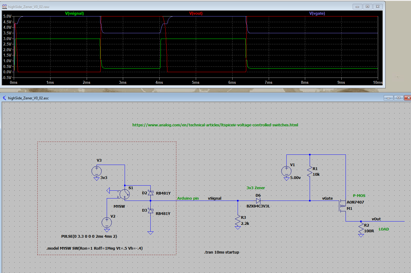
Yes, I did mention the pin protection diodes but here is another "solution" based as best as I can on bits from LTSPICE using a voltage controlled switch to simulate the pin switch between 3v3 and high impedance (INPUT). In principle it uses a 1n4148 diode to allow the mosfet gate to rise to 5v to switch it off.
@6v6gt@ShermanP I am not really sure of how the internal GPIOs work in INPUT mode. I just know that the pins can be set to either INPUT, INPUT_PULLUP or INPUT_PULLDOWN mode on the ESP32. The latter two supposedly create a simple pullup/pulldown equivalent circuit.
I saw a nice schematic here for a regular transistor and 5V GPIO: http://lednique.com/gpio-high-side-driver-fail/
which explains nicely what @shermanP was talking about (although the equivalent schematic seems to depict the pin in OUTPUT mode).
@6v6gt wouldn't D1 from your schematic just let that type of current pass through? Your simulation seems to show that the switching between OUTPUT HIGH and INPUT does trigger the PMOS but I guess I don't really understand how the path in red on the schematic above is prevented.
It is so that I made an error in that I did not model the pin protection diodes correctly so the results are misleading.
Assuming two Schottky diodes, the circuit would be something like this. However, the best solution is the one that you have now implemented with the NPN transistor.
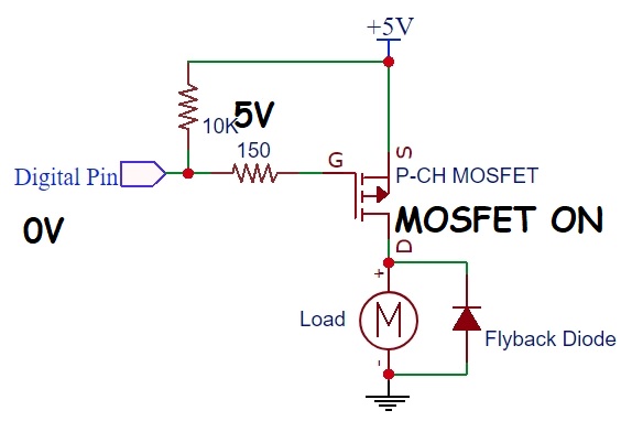
I am not an expert in transistors, but as far as I understand, when the input is low, the transistor is an open switch, so 5V is connected to PMOS Gate through 10k+150k. (making V(gs)=0V?) When the input is high, the transistor acts as a wire shorting the midpoint between 10k and 150R to ground, pulling G to 0V and creating a V(gs) to trigger the PMOS. I might be wrong.
From schematic in post #3. when digital pin is high, 2N3904 is on, which pulls p-ch gate to 0V. VGS is voltage at gate minus source = 0v - 5v = -5v. -5v is below the threshold voltage, which turns mosfet on.
When digital pin is low, 2N3904 is off and gate of p-ch is pulled to +5V through the 10k pullup resistor. VGS = 5v - 5v = 0v. 0v is above the threshold voltage, so mosfet is off.