I'm using an ADS1115 to measure the characteristaics of a three terminal device. In this example a 4N35.
This is the circuit
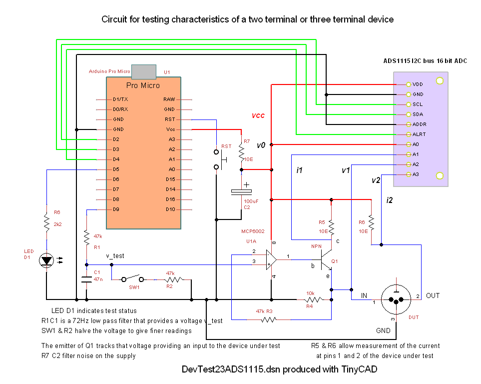
A0 measures Vcc
A1 measures i1 using A0-A1 differential
A2 measures V1
A3 measures V2 and A0 - A3 measures i2
I cant use differential mode because it only works on A0-A1 or A2-A3.
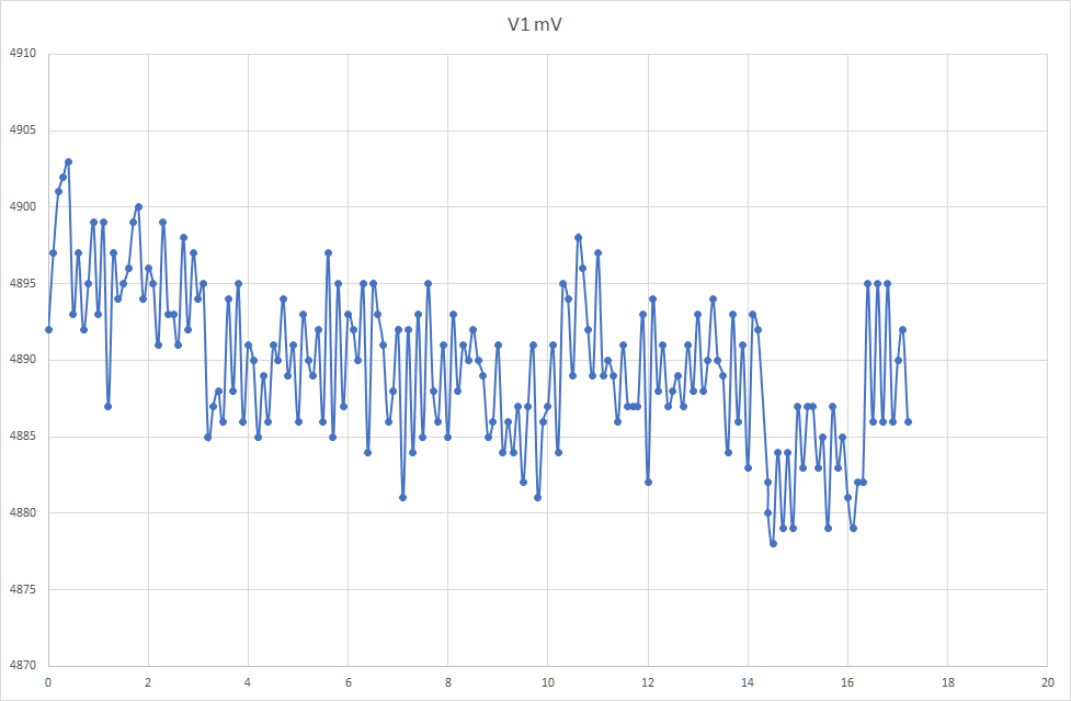
Annoyingly, I'm seeing a lot of noise on the reading for i2 - which I believe is indicative of noise on the GND-Vcc supply; but I've put an RC filter on with little if any improvement.
I've considered the layout; Vdd, A0, C2+ R5 and R6 are all on the same track.
The noise on the i2 measurement is still present if T2 of the DUT is disconnected.
Example data: the 0.019mV on iDUT is 1 lsb so ignore. The 0.356mV on iT3 is 19 lsb.
| nOut | vDUT | iDUT | iT3 | vT3 |
|---|---|---|---|---|
| 0 | 22.7 | 0 | 0 | 5031.7 |
| 2 | 22.7 | 0 | 0 | 5030.1 |
| 4 | 36.4 | 0 | 0.356 | 5027.2 |
| 6 | 55.5 | 0 | 0 | 5027.2 |
| 8 | 75 | 0 | 0 | 5028 |
| 10 | 95.1 | 0.019 | 0 | 5029.7 |
| 12 | 114.9 | 0.019 | 0.356 | 5025.6 |
| 14 | 135.2 | 0 | 0 | 5026.5 |
| 16 | 155.6 | 0 | 0 | 5027.1 |
| 18 | 175.9 | 0 | 0.056 | 5027.2 |
| 20 | 196.1 | 0 | 0 | 5029.5 |
| 22 | 216.4 | 0.019 | 0.056 | 5028.7 |
| 24 | 236.4 | 0 | 0.038 | 5026.1 |
Here is the code (sorry there's a lot of commented out)
#include <Adafruit_ADS1X15.h>
//modified from example because Micro Pro uses different pins for scl & sda
// The library has 'getDataRate' and 'setDataRate' commands. Use them to check the sampling rate and set another.

/*
*** Micro Pro and ADS1115 used for testing two (2) terminal or three (3) terminal devices.
*** generates a voltage using a fast PWM wave at 31kHz and RC filter
*** buffers the voltage with an op amp and emitter follower
*** measures device voltage and device current
*** see diagrams rropamptest ads1115.dsn && devtest23ADS1115.dsn tinyCAD
*** skillbank March 2023
*/

Adafruit_ADS1115 ads; /* Use this for the 16-bit version */
//Adafruit_ADS1015 ads;     /* Use this for the 12-bit version */

#define RATE_ADS1115_8SPS (0x0000)    ///< 8 samples per second
#define RATE_ADS1115_16SPS (0x0020)   ///< 16 samples per second
#define RATE_ADS1115_32SPS (0x0040)   ///< 32 samples per second
#define RATE_ADS1115_64SPS (0x0060)   ///< 64 samples per second
#define RATE_ADS1115_128SPS (0x0080)  ///< 128 samples per second (default)
#define RATE_ADS1115_250SPS (0x00A0)  ///< 250 samples per second
#define RATE_ADS1115_475SPS (0x00C0)  ///< 475 samples per second
#define RATE_ADS1115_860SPS (0x00E0)  ///< 860 samples per second

//SDA to D2 and SCL to D3; ALERT to D4; ADDR not connected
// Pin connected to the ALERT/RDY signal for new sample notification.
constexpr int READY_PIN = 4;


//state indicator
byte LED = 5;    //LED on pin 5
bool ON = HIGH;  //LED is ON when pin is HIGH
bool OFF = LOW;


//generating PWM signal
constexpr byte vOutPin = 9;  // using pin 9 for pwm out
const int divider = 1;  //PWM: for pin 9 divider=1 sets pwm freq at 31,250Hz; = 8 sets it to 3,906Hz
//with emitter follower compliance runs out at 4400mV approx
int nMax = 225;     // value is the duty cycle of the pwm ie 255 = always 1, 0 = always off.  2v5=128
int nMin = 000;     //0 to start at 0V
int stepSize = 2;   //each step is an increment of about 20mV at DUT

int nOut;           //number to be output via PWM
int tSettle = 200;  //msec to allow PWM to stabilise

//calculating expected output voltage at filter
float mVoltsOut;
//vCal calibrates the indication of output voltage in mV
//float vCal = 19.53;  // mV out = nOut * Vcc mV / 256  5000 /256 = 19.53
float vCal = 19.5;  //mV out - from EXCEL trend line
int vOffset = 12;   // mV out - from EXCEL trend line

//measuring current
int tInt = 4; //interval between readings
int rIsense = 10;  //value of current measuring resistor
int rIsense3 = 10;  //value of current measuring resistor for T3
float iDUT;        //current in device under test
float iT3;        //current through terminal 3 eg collector of transistor
float iDUTthreshold = 0.04; //current (mA) above which finer steps will be taken note 0.019 or 0.038 is noise level
float iT3threshold = 0.1; //current (mA) above which finer steps will be taken
//*** threshold - take fewer readings below threshold to reduce unnecessary data

int iLimit = 20;   //end test when iLimit is reached


void setPwmFrequency(int pin, int divisor);

// This is required on ESP32 to put the ISR in IRAM. Define as
// empty for other platforms. Be careful - other platforms may have
// other requirements.
#ifndef IRAM_ATTR
#define IRAM_ATTR
#endif

volatile bool new_data = false;
void IRAM_ATTR NewDataReadyISR() {
  new_data = true;
}

void setup(void) {
  Serial.begin(115200);
  pinMode(LED, OUTPUT);  //led & resistor on pin 5 to show test status
  Serial.println("Starting test on device");
  digitalWrite(LED, ON);       //LED on, pause before test starts
  analogWrite(vOutPin, nMin);  //generate minimum voltage for test
  delay(4000);                 //time to allow vout to settle to vMin, and start serial monitor (termite, needs cts/rts)
  Serial.println("Getting single-ended readings from AIN0..3");
  Serial.println("ADC Range: +/- 6.144V (1 bit = 3mV/ADS1015, 0.1875mV/ADS1115)");

  // The ADC input range (or gain) can be changed via the following
  // functions, but be careful never to exceed VDD +0.3V max, or to
  // exceed the upper and lower limits if you adjust the input range!
  // Setting these values incorrectly may destroy your ADC!
  //                                                                ADS1015  ADS1115
  //                                                                -------  -------
  ads.setGain(GAIN_TWOTHIRDS);  // 2/3x gain +/- 6.144V  1 bit = 3mV      0.1875mV (default)
  // ads.setGain(GAIN_ONE);        // 1x gain   +/- 4.096V  1 bit = 2mV      0.125mV
  // ads.setGain(GAIN_TWO);        // 2x gain   +/- 2.048V  1 bit = 1mV      0.0625mV
  // ads.setGain(GAIN_FOUR);       // 4x gain   +/- 1.024V  1 bit = 0.5mV    0.03125mV
  // ads.setGain(GAIN_EIGHT);      // 8x gain   +/- 0.512V  1 bit = 0.25mV   0.015625mV
  // ads.setGain(GAIN_SIXTEEN);    // 16x gain  +/- 0.256V  1 bit = 0.125mV  0.0078125mV

  if (!ads.begin()) {
    Serial.println("Failed to initialize ADS.");
    while (1)
      ;
  }
  ads.setDataRate(RATE_ADS1115_8SPS);
  //ads.setDataRate(RATE_ADS1115_64SPS ); //choose either
  setPwmFrequency(vOutPin, divider);
  Serial.println("Testing device with rail-rail op amp: generating vOut, measuring vIn");

  //turn off built in LEDs by setting them as inputs
  pinMode(LED_BUILTIN_TX, INPUT);
  pinMode(LED_BUILTIN_RX, INPUT);
}

void loop(void) {
  int16_t adc0, adc1, adc2, adc3;
  float multiplier = 0.1875F; /* ADS1115  @ +/- 6.144V gain (16-bit results) */
  //voltages need to be floats or we lose resolution on iDUT as v2-v1/rIsense
  //float volts0, volts1, volts2, volts3;
  float mVolts0, mVolts1, mVolts2, mVolts3;
  float vDiff, vDiff3;  //difference between two readings
  delay(500);   //time to allow vout to settle to zero and
  //Serial.println("nOut, mVoltsOut, vFilter, vDUT, vIsense, Vsupply, vDiff,  iDUT");
  //Serial.println("nOut, mVoltsOut, vDUT, iDUT, Vload, Iload");
  Serial.println("nOut, vDUT, iDUT, iT3, vT3");
  digitalWrite(LED, OFF);  //LED off, test in progress

  for (nOut = nMin; nOut <= nMax; nOut += stepSize) {
   // for (nOut = nMax;;){  //used for full scale calibration
    //for (nOut = 0;;){  //used for offset null
    //for (nOut = 64;;){  //used for freq measurement

    analogWrite(vOutPin, nOut);  //set output voltage; having set the pwm frequency the analog write obeys that
        delay(tSettle);

    //calculate expected output voltage at filter
    mVoltsOut = (nOut * vCal) + vOffset;

    // Serial.print(mVoltsOut, 1);
    //Serial.print(",   ");

    //take numeric readings from adc and convert to mV
    adc0 = ads.readADC_SingleEnded(0);  //supply voltage
    mVolts0 = adc0 * multiplier;
    delay(tInt);
    adc1 = ads.readADC_SingleEnded(1);
    if(adc1 > adc0) adc1 = adc0; //cant be higher voltage than supply
    mVolts1 = adc1 * multiplier;
    delay(tInt);
    adc2 = ads.readADC_SingleEnded(2);
    mVolts2 = adc2 * multiplier;
    delay(tInt);
    adc3 = ads.readADC_SingleEnded(3);
    if(adc3 > adc0) adc3 = adc0; //cant be higher voltage than supply
    mVolts3 = adc3 * multiplier;
    delay(tInt);
    vDiff = ads.readADC_Differential_0_1();
    vDiff *= multiplier;  //calculate difference voltage in mV between supply and ISense
    //calculate current
    iDUT = vDiff / rIsense;  //

    vDiff3 = mVolts0 - mVolts3;
    iT3 = vDiff3 / rIsense3;


    //*** print results in .csv format:- only need vDUT vs iDUT to plot characteristic
    Serial.print(nOut);
    Serial.print(",  ");
    /*
    //Diagnostic - used while testing
    Serial.print("V supp:   ");
    Serial.print(mVolts0, 0);  //Vsupply
    Serial.print(",   ");

    Serial.print("V rIsense: ");
    Serial.print(mVolts1, 1);  //v DUT output
    Serial.print(",   ");
*/
    //Serial.print("vDUT:  ");
    Serial.print(mVolts2, 1);  //
    Serial.print(",   ");

    //Serial.print("iDUT:  ");
    Serial.print(iDUT, 3);  //current mA
    Serial.print(",   ");

    //Serial.print("iT3:  ");
    Serial.print(iT3, 3);  //T3 current mA
    Serial.print(",   ");

    //Serial.print("Vt3: ");
    Serial.print(mVolts3, 1);  //Vterminal2
    Serial.print(",   ");


    //Serial.print("adc0 raw:  ");
    Serial.print(adc0);  //
    Serial.print(",   ");

    //Serial.print("adc1 raw:  ");
    Serial.print(adc1);  //
    Serial.print(",   ");

    //Serial.print("adc2 raw:  ");
    Serial.print(adc2);  //
    Serial.print(",   ");

    //Serial.print("adc3 raw:  ");
    Serial.print(adc3);  //
    Serial.print(",   ");

  //  Serial.print("vDiff:  ");
  //  Serial.print(vDiff, 2);  //Vdifference
  //  Serial.print(",   ");


     Serial.println();  // end of one line of data
    //test if getting useful data
    if (iDUT > iDUTthreshold) {
    //  if ((iDUT > iDUTthreshold)||(iT3 > iT3threshold)) {
      stepSize = 1;
    }

    if ((iDUT > iLimit)||(iT3 > iLimit)) {
      nOut = 0;
      Serial.println("current limit exceeded, terminating test");
      analogWrite(vOutPin, nOut);  //*** NB turn off voltage to device so as not to leave it stressed
      break;
    }
  }                         //finished test
  while (1) {               //flash LED to show test finished
    digitalWrite(LED, ON);  //LED on,
    delay(50);
    digitalWrite(LED, OFF);  //LED on,
    delay(1000);
  }
}

/**
   Divides a given PWM pin frequency by a divisor.

   The resulting frequency is equal to the base frequency divided by
   the given divisor:
     - Base frequencies:
        o The base frequency for pins 3, 9, 10, and 11 is 31250 Hz.
        o The base frequency for pins 5 and 6 is 62500 Hz.
     - Divisors:
        o The divisors available on pins 5, 6, 9 and 10 are: 1, 8, 64,
          256, and 1024.
        o The divisors available on pins 3 and 11 are: 1, 8, 32, 64,
          128, 256, and 1024.

   PWM frequencies are tied together in pairs of pins. If one in a
   pair is changed, the other is also changed to match:
     - Pins 5 and 6 are paired on timer0
     - Pins 9 and 10 are paired on timer1
     - Pins 3 and 11 are paired on timer2

   Note that this function will have side effects on anything else
   that uses timers:
     - Changes on pins 3, 5, 6, or 11 may cause the delay() and
       millis() functions to stop working. Other timing-related
       functions may also be affected.
     - Changes on pins 9 or 10 will cause the Servo library to function
       incorrectly.

   Thanks to macegr of the Arduino forums for his documentation of the
   PWM frequency divisors. His post can be viewed at:
     https://forum.arduino.cc/index.php?topic=16612#msg121031
*/
void setPwmFrequency(int pin, int divisor) {
  byte mode;
  if (pin == 5 || pin == 6 || pin == 9 || pin == 10) {
    switch (divisor) {
      case 1: mode = 0x01; break;
      case 8: mode = 0x02; break;
      case 64: mode = 0x03; break;
      case 256: mode = 0x04; break;
      case 1024: mode = 0x05; break;
      default: return;
    }
    if (pin == 5 || pin == 6) {
      TCCR0B = TCCR0B & 0b11111000 | mode;
    } else {
      TCCR1B = TCCR1B & 0b11111000 | mode;
    }
  }
}