larryd:
If you have ordered PCBs with cutouts inside your board, what was your process to do so?
What board manufacturer did you use?
Did you need to inform the factory ahead of time about the cutout?
For simple slots have you ever used closely spaced holes of appropriate size?
We have on the rare occasion had to do something like that to customer boards. I use the resharpened carbide drill bits and burrs used for fr4 circuit boards. I guess they are still available on Ebay. They have 1/8 inch shafts.
I have a Dumore drill press that will turn 0 to 10,000 rpm or 0-30,000 rpm. I use the burr or drill bit in the Dumore and put the circuit board on a sacrificial piece of board and start cutting.
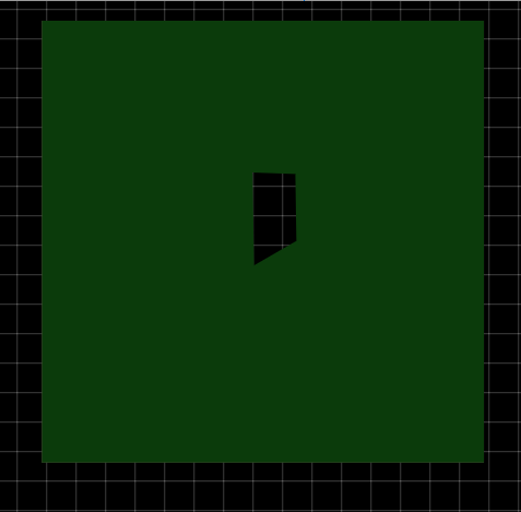
This issue crops up when you need a board footprint for something like a 5.5mm/2.5mm power socket. The connector requires through hole plated slots in the PCB.
I sent a PCB off to one of the standard suppliers, $10 for 10 off 10cm x 10cm PCBs, and it came back slotted, I had not realised the connector footprint on the PCB had slots on the milling layer (it was not one on my designs).
Just recently I had a PCB done, with a different supplier, using the same PCB footprint. So I assumed it would come back slotted. It did not.
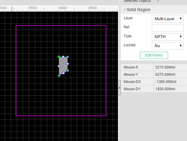
I use OSH Park. They are fine with any oddly-shaped cutouts anywhere on the board. There are some restrictions that are clearly documented on their website.
I just draw the cutouts on the outline layer with zero-width lines.
The one thing they won't do is plated slots, such as are required for the barrel connector on the UNO.
I use the edge layer in KiCAD for e.g. slots between mains and low voltage parts. Always came back right from Seeed and JLC without any additional interaction. It also displays correctly in their Gerber viewer.