No ground plane needed.
I would include one, why do you think a ground plane is not needed? No cost to including one, is there any potential problem in doing so?
Since there are next to no traces on the component side placing a GND pour on the foil (bottom) side might make manufacturing difficult as the electroplating currents will be unbalanced.
![]()
Forgive me if I already asked, did you allow sufficient clearance for the USB plug to attach to the module?
I'm not entirely sure what you mean. The Teensy is going to be on 2x14pins header so it should be easy to connect the USB.
Some headers are nearly flush with the board. I've occasionally had situations where the USB plug was too big and hit something, I had to go hunt for a smaller one to make it possible to insert.
Since then, I've always placed the USB connector flush with the motherboard edge. It helps also, in the case where you mount the board inside an enclosure and expose the USB connector to the outside.
Here is my messy layout ![]() :
:

The black cables are Serial I/O, the dashed lines are the power supply/ground, the grey ones are the communication pins and each brown,green,red cable is for one potentiometer.
Well, I can also keep in good humour. ![]() But I will never, ever try to read something like that. Is there some reason you can't make a real schematic?
But I will never, ever try to read something like that. Is there some reason you can't make a real schematic?
whoops. ![]() I thought you wanted to see the placement of the PCBs at the front plate. I'll make a schematic and post it.
I thought you wanted to see the placement of the PCBs at the front plate. I'll make a schematic and post it. ![]()
I've lost track. Maybe your problem is already solved. But a schematic ought to exist for yourself and anyone that has to deal with the circuit. It is not just for the benefit of forum readers...
My last question was strictly about physical dimensions. So it has nothing to do with schematics.
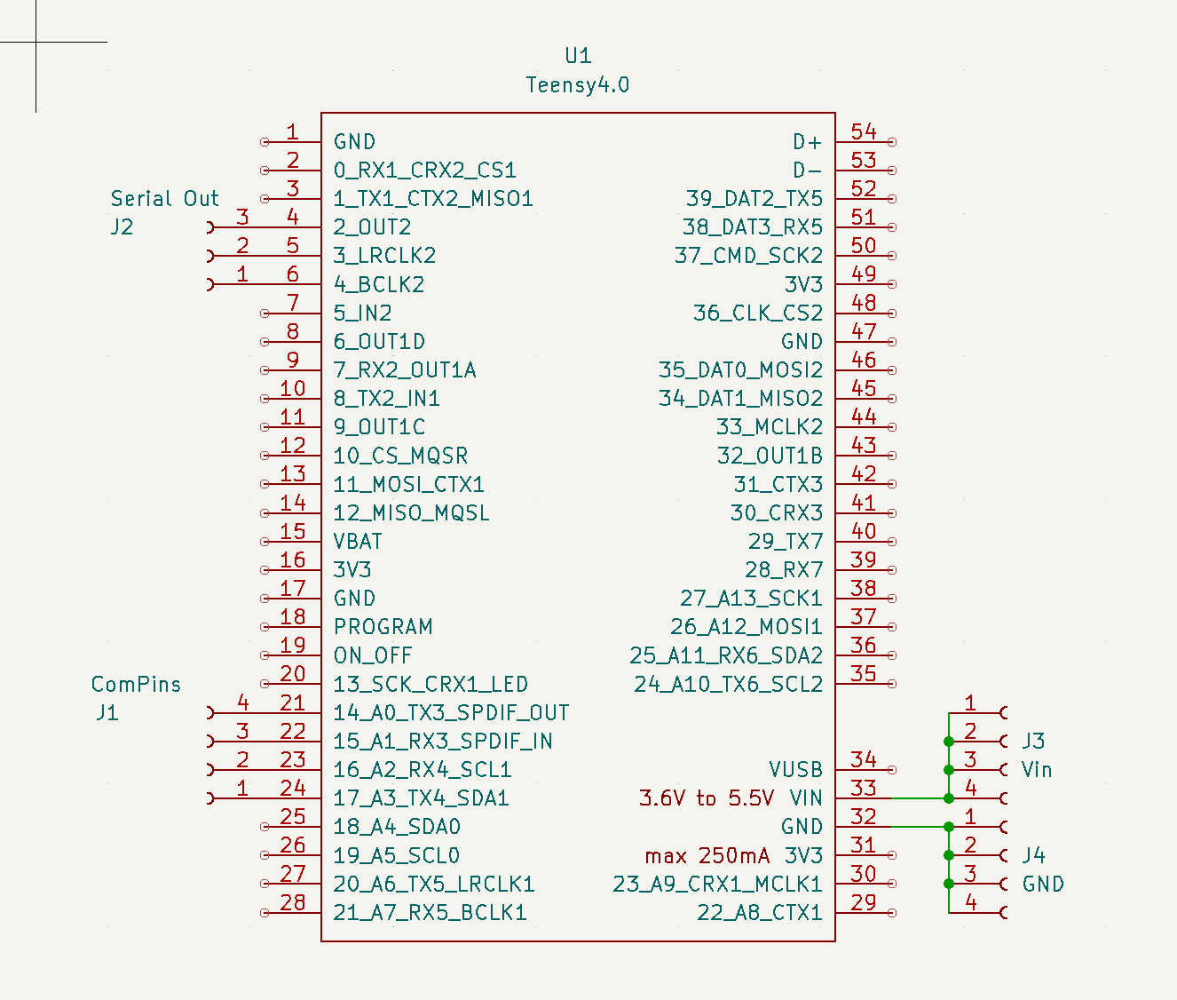
Here are the schematics of the main module and the multiplexer modul of which I'm going to have four.

This topic was automatically closed 180 days after the last reply. New replies are no longer allowed.