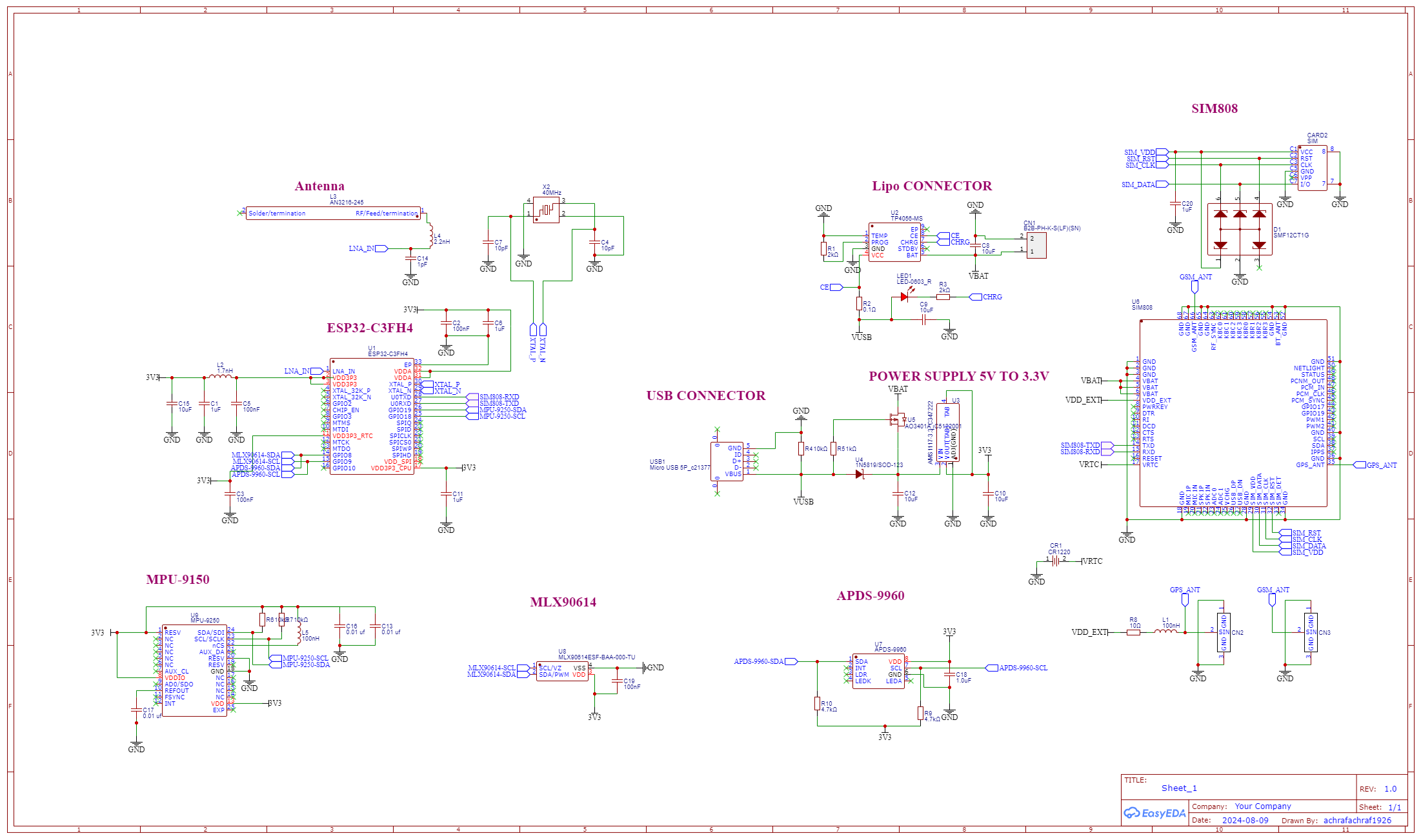
Why are you using three separate I2C buses? Why not have all sensors on the same bus? Is there some kind of inherent address conflict that cannot be resolved?
The pullups are on the weak side but on a board as small as this will likely be OK. I'd drop them to 3k3 though.

Why not use a Schottky diode here with a lower forward voltage drop? This one leaves your AMS1117 starved. Dropout voltage is up to 1.3V for this type; this means you need 4.6V input for reliable 3.3V output. The selected diode leaves roughly this, maybe slightly less, and if your USB voltage happens to be slightly lower than 5V it'll become a marginal affair for sure.

What's the purpose of R2?

How does the 1pF of C14 relate to the parasitic capacitance of the associated traces and pins/pads? 1pF is awfully little; the traces between the ESP32 and the antenna circuit seem awkwardly long; refer to a commercially made ESP32 board to see how it's done. Also refer to the datasheet of your antenna chip for layout guidelines. It seems like your design violates all recommendations.
In all honesty, I'd recommend using an ESP32 module that already has the antenna included on its PCB. This saves you the trouble of undertaking a tricky bit of HF design. Your own design may not work at all, or may have very poor range, and/or may be inadvertently very directional.

Are you sure you want to power the SIM808 from battery even if USB power is available?
Where are the decoupling capacitors for the SIM808 module?
Where are the 22R series resistors between the SIM808 and the SIM card module?
How have you determined correct physical layout of the antenna circuit on the SIM808? Where are the matching components as described on page 53 of the datasheet?
Points above: see SIM808 datasheet
The PCB layout I find hard to read. I'm wondering why you have components on both sides. Is there a space constraint that forces you to do this? Even so, are you sure it won't fit all on one side? There's a lot of empty space. Component placement in general I feel is far from optimal and in some cases (where it concerns RF) in violation of guidelines laid out in datasheets of components used, does not appear to keep into account tuning of antenna circuits etc.
Keep in mind when mounting somewhat bigger parts (battery holder, sim card holder) on the bottom of the PCB, this may affect the possibilities of physically mounting the PCB into its housing; clearance can become an issue.
Your power traces are very thin. They'll work in principle, but best practice is to make them a little heavier. Go with 1mm or heavier wherever this is physically possible. An ESP32 with radio on can draw several hundred mA. The SIM808 can draw peak currents of 2A. I see no provisions on your board for these peak currents.
Add some buffer capacitance on the board; 47-100uF should be OK. Near the USB connector would be a nice spot. Use an aluminum electrolytic.
Overall, there's much room for improvement. But I also think you're biting off far more than you can chew by working on a board that involves several RF circuits that require specialized knowledge w.r.t. component selection, physical layout. I suspect you also do not have the equipment required to perform the necessary testing how well your RF designs function. Instead of this bare-metal approach, I would recommend using ready-made modules for the RF parts so that you can rely on pre-made circuitry that can be safely assumed to perform well.