Is this a tree layer board?
That would be super odd.
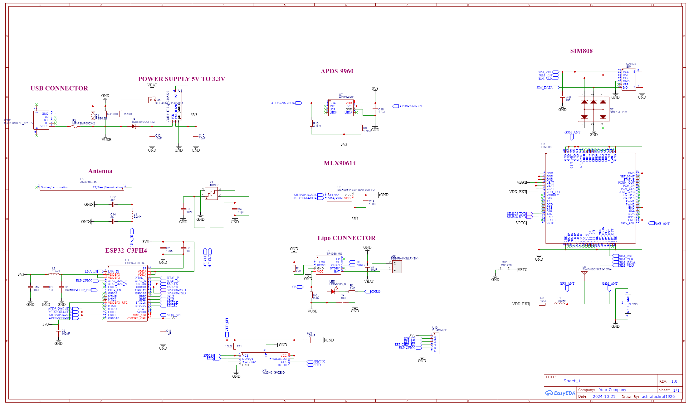
Schematic:
USB connector shield is not grounded.
Press 'y' to flip the connector, ground is usually placed below Vcc. It's odd to look up for Vcc below the components.
I usually place the power bank (every single cap between Vcc and ground) in some other place.
You forgot to place grounded holes. If possible, check for test points.
So, one good practice is to place, for every part/IC inputs at its left, outputs at its right. That's not always possible, but it will improve reading of the schematic. Also placing Vcc always above the component, GND below the component.
PCB: What is green? Is a 3rd layer? That would be odd.
Holes are usually grounded, they should be placed in the schematic (grounded via).
Why all designators are flipped? Place them properly. Some of them are not even inside the board.
There is a trace that might give some trouble, super close to the edge of the board. Never do that.
I understand that you have two connectors (left down). They are super close. It will be really hard to pull the cable out (things might look big on screen, but they are really small). Give them some space.
If green is a 3rd layer board, 4th layer should be ground.
Also, you dont fill with ground your designn, is there any reason?
Mounting holes are super close to the edges.
I'm not an expert, but I remember when I started oon this I commit the same mistakes. I wanted everything to fit in a super mall PCB. That wont work, you are spending money for premium design, and it wont work, you will not be able to debug it (because is super tiny).
Make the board bigger, never go for minimum track width or minimum track clearance. Make tracks super fat, 0.5 minimum. 0.75/1mm for Vcc.
Vcc caps should be always right before the Vcc input pin.
Vcc supply -> + Cap -> Vcc input.