I have designed a few PCBs so far and they work alright. They are digital circuits with a microcontroller and sometimes with an analog voltage input or a sensor input, etc. Nothing too fancy, nothing too fast.
And this is how I always do my PCB grounding (black fill = GND):
I leave that thick edge because I etch myself and by experience it works better this way. And I fill everywhere else with GND. Because:
1- Components will have easy access to GND
2- I won't have to worry about the GND trace being too narrow for high currents
3- It works as a heat sink
4- It shields against EMI
5- Less acid will be used for etching
Now every time I do an actual research I end up with very confusing and sometimes contradictory information about how a PCB ground should be done.
Some say it has to be like a star topology with only one path from any component to GND.
Some say a ground plane should be used (isn't a ground plane equal to infinite paths to GND?).
Some say ground should be separated for analog and digital parts of the circuit.
Some say a ground fill like I do should be used.
Some say a ground fill is bad and should be avoided.
Some say a ground fill doesn't shield against EMI at all.
etc. etc...
And there's a lot of stuff about current return path that I don't understand. And any tutorial I've found online is too advanced and uses concepts I don't understand.
So I was wondering if anyone could explain to me how exactly I should do my grounds because I'm just hopelessly confused about it.
I know it will be different based on how many layers I have so please explain for one layer PCB (like the pics) and two layer PCB. As it will be unlikely I'll ever use anything else.
Or if you know a source I can read to understand it, that would also be much appreciated. Mind that I don't have formal electronics background so the source will have to explain the basics as well.
larryd:
At the frequencies and complexity that a hobbyist is usually using a ground pour similar to yours is sufficient.
I've actually asked a similar question on this forum before and this was the general idea that I got from everyone's answers. Hence going on with the ground fill design.
However every time I stumble upon the topic I see stuff that confuses me.
What made me make this similar thread again was a few PCB design guide I just read and this stack exchange question.
The OP is making an LCD display with an Arduino. Nothing fancy I'd say. But the top answer is basically saying that ground traces are better than ground fill. How can that be possible? With ground fill you have ground everywhere, it's basically infinite traces.
Looks like you can reduce the GND clearances, will help to completely cover the board.
I did experiments and this is the safest clearance to use when etching (I etch myself with acid).
Make sure you add proper power supply decoupling for all I.C.s.
Oh I do a whole lot of that. If anything I overdo it.
Thanks for the video link, will take a look.
pourduino:
Now every time I do an actual research I end up with very confusing and sometimes contradictory information about how a PCB ground should be done.
Some say it has to be like a star topology with only one path from any component to GND.
That's for low frequency precision analog stuff.
Some say a ground plane should be used (isn't a ground plane equal to infinite paths to GND?).
For any high frequency stuff (including high speed logic).
Some say ground should be separated for analog and digital parts of the circuit.
For precision analog in mixed-signal situation - ie ADCs and DACs
Some say a ground fill like I do should be used.
Some say a ground fill is bad and should be avoided.
Some say a ground fill doesn't shield against EMI at all.
Groundplane definitely reduces coupling between parts of the circuit, but doesn't
eliminate it - that takes shielded boxes. But the reduction is always going to help
avoid risks of oscillation and cross-talk.
etc. etc...
And there's a lot of stuff about current return path that I don't understand. And any tutorial I've found online is too advanced and uses concepts I don't understand.
At high frequecies the return path follows the signal, requiring a groundplane when there are
lots of fast signals to toure, otherwise you'd need a return ground wire for every signal wire.
You may notice that at low frequencies the rules are different - this is because at low frequencies
only the resistances matter - and these tend to only cause very small error voltages, hence they
matter only for precision analog stuff (including high gain audio amps for instance)
At very high frequencies stray inductance and capacitance, and transmission-line effects completely
dominate everything - as you get to microwave frequencies you have to treat everything as a
wave propagating down a transmission line, pretty much.
At intermediate frequencies you can get away with less concessions to RF design, but it depends
on the circuit impedance as well as the frequencies involved. Higher impedance, higher frequencies
both lead to stray inductance and capacitange mattering more.
pourduino:
Some say it has to be like a star topology with only one path from any component to GND.
As Mark points out, that would be the case for a very limited number of parts and specific areas in very rare instances of analog circuits only. In almost all cases, using the ground fill to provide multiple paths for ground returns to minimise resistance and inductance is better, and an actual ground plane - separate layer - best.
pourduino:
Some say a ground plane should be used (isn't a ground plane equal to infinite paths to GND?).
If you are able to dedicate the third board layer for this purpose. As with essentially all computer motherboards.
pourduino:
Some say a ground fill is bad and should be avoided.
It would be difficult indeed to argue that, except exclusively for particular regions where it is critical to minimise capacitance. That said, you obviously do not use ground fill for high voltage areas including power mains.
I notice there are areas of the board patterns you illustrated that you chose not to use ground fill for some reason.
larryd:
Since you are making SS boards, it’s my guess you are having success with your current methods and you are just overthinking things too much.
I do tend to overthink things. Sometimes quite compulsively. I need to listen to your advice.
But on the other hand I hate it when I read something online that contradicts what I thought was true.
New knowledge is fine, but when you think you know how to do PCB ground and then you read something that makes you think you've been doing it all wrong this whole time, that really irritates me.
MarkT:
At high frequecies the return path follows the signal, requiring a groundplane when there are lots of fast signals to toure, otherwise you'd need a return ground wire for every signal wire.
I think this is the thing that I'm not quite getting about return paths.
So say I have an 8-pin IC. It has a VCC pin, a GND pin, 3 input pins and 3 output pins.
This IC is connected to a microcontroller. And everything is being powered from a power supply.
If I do have a dedicated ground plane then all high speed/AC current returns will automatically travel right underneath their signal traces because it has the least impedance.
But if I don't have a ground plane, what does it mean to create a return ground wire for every signal wire?
Does this mean I need something like this? (Imagine this is the actual PCB not a diagram):
This is the only thing I can imagine when people say high speed signal traces need their own return trace.
If this is the case then I can see how not having an actual dedicated ground plane can be a problem here. Because you can't connect Q2 and Q1 to IN2 and IN3 AND have that kind of return trace unless you have a layer underneath.
Paul__B:
I notice there are areas of the board patterns you illustrated that you chose not to use ground fill for some reason.
Ah yes, the first one is because I didn't want to have ground underneath the ESP's antenna, and the second one is because my clearances are thicker than usual so the ground fill can't find a way in through the holes.
pourduino:
This is the only thing I can imagine when people say high speed signal traces need their own return trace.
If this is the case then I can see how not having an actual dedicated ground plane can be a problem here. Because you can't connect Q2 and Q1 to IN2 and IN3 AND have that kind of return trace unless you have a layer underneath.
But that is not a high speed signal trace, so it is simply not relevant.
If you were having high speed signal traces, two things would happen. One is that you would have a ground plane, and the other is that the ICs themselves would be designed to provide for the necessary shielding grounds.
pourduino:
Ah yes, the first one is because I didn't want to have ground underneath the ESP's antenna, and the second one is because my clearances are thicker than usual so the ground fill can't find a way in through the holes.
Then your design has failed in the first case. It is not a matter of not having ground under the ESP antenna, it is a matter of positioning the antenna so that there is no surrounding conductor at all within at least a wavelength.
If using ESP modules, you need to arrange it so that the antenna section completely overhangs beyond the motherboard. However, correctly spaced, a solid metal plane would direct the radiation pattern and provide gain.
As to the second design, it does appear that slight re-routing would have allowed many further areas to be ground filled, FWIW.
Paul__B:
It is not a matter of not having ground under the ESP antenna, it is a matter of positioning the antenna so that there is no surrounding conductor at all within at least a wavelength.
But that's 12cm! :o
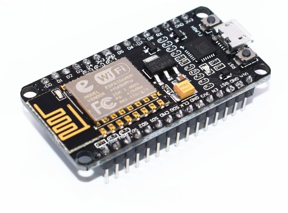
Also even in NodeMCU boards it's not sticking out as you suggested:
Well, I did deliberately add the caveat "surrounding".
I would say that your continuous loop of ground around your deliberately open area is seen at this wavelength, as pretty much the same as a solid plane and will substantially reduce if not eliminate radiation in the direction through your motherboard.
pourduino:
Also even in NodeMCU boards it's not sticking out as you suggested:
Ah, but in fact, it is.
It is clearly open in all directions but one. But if you mount the board to something conductive, you will shield it from that direction - and may de-tune the antenna as well. It's just basic radio stuff I am afraid.
Paul__B:
Well, I did deliberately add the caveat "surrounding".
I would say that your continuous loop of ground around your deliberately open area is seen at this wavelength, as pretty much the same as a solid plane and will substantially reduce if not eliminate radiation in the direction through your motherboard.
That was extremely informative! Thank you.
I'm very happy that I watched the video suggested by @larryd before reading that because they were very related.
I learned so much from making this thread. Thanks everyone.