Stair occupancy using force sensors, part 2

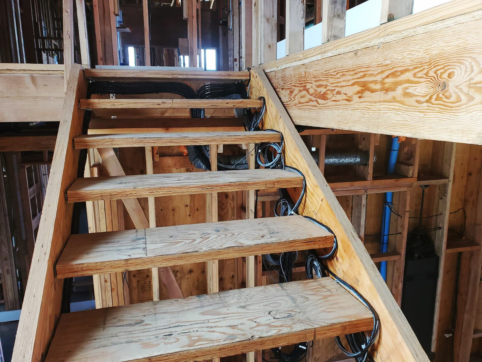
Almost a year ago I posted a thread about using force sensors to detect when stairs are stepped on so I can animate the LED strip in each of 16 stairs. I got it working, soldered up in a protoboard, but it wasn't pretty. Since then I've improved it a lot, so I wanted to show off the new solution and also give special thanks to @DaveEvans for sticking with me so long as I struggled through learning and getting things working.

First, I can make a proper schematic now!

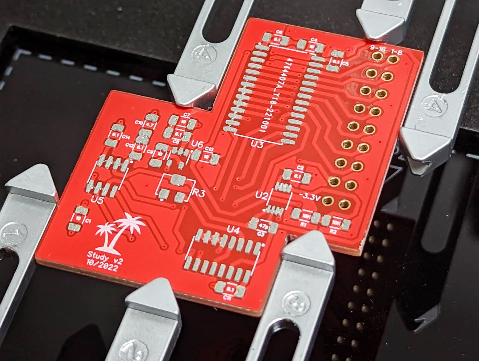
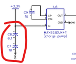
I improved the design slightly since the protoboard by replacing a 100K resistor with a 200K trimmer. This resistance controls the sensitivity of the sensors, ie how quickly they reach the max range of the ADC. The trimmer gives fixed resistance that's the same for all 16 stairs. I also have 200K from a digital potentiometer, so that can differ per stair, if needed. My total range is ~1K to ~400K. Testing shows ~200K works well to detect a person stepping on a stair, but we'll see in the actual installation.

Onward to building my new, fancy solution:
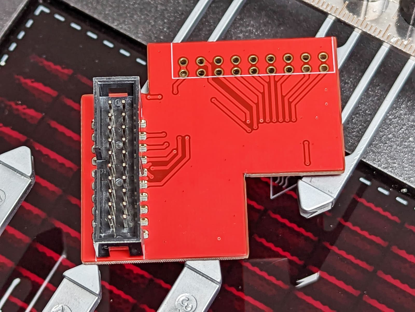
And the back:

I tried to learn KiCAD, but I just don't like it. Eventually I found DipTrace. While it has its quirks, I'm much more productive with that. I came back later and tried KiCAD again, but I find there are many minor UI annoyances and I didn't find it easy to create my own footprints, so I'll stick with DipTrace.

Next I needed a box for my wESP32 and PCB, so I designed one in SketchUp and got it printed by JLCPCB (who also made the PCB):

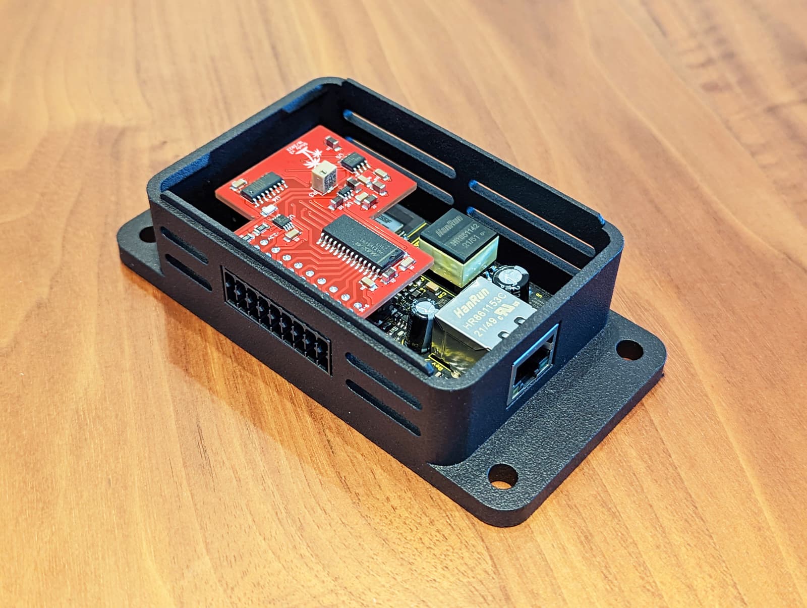
The 3D print is MJF with PA12-HP nylon. The cost was ~$35 for the box, plus shipping. Not cheap, but it is really nice, with a light texture. It's difficult to even tell it's 3D printed. One downside is MJF sometimes has light streaks on large flat surfaces. Thankfully this was never a problem for my prints. It was very helpful for designing my enclosure to use DipTrace to export a 3D model of the PCB. It's great to be able to just snap the wESP32 into the box, plug in the PCB, snap on the lid, and it's done! No wires, no screws. Maybe the best part is if I need to redesign or otherwise replace the PCB or wESP32, I just order a new one and swap it out. This pic shows the wESP32 clips:

The top clips are fixed, the bottom ones are flexible. The lid also snaps on/off, that worked out great, with no play.

The house is still being built, so sadly I can't yet show the LED strips in action yet, I can only show the brains, above. I'll come back and show it when it's finished! The software is ready though and the initial animation will work like this:

stairs

The stair LED strips are controlled by DMX, so I don't need to deal with that directly. My little box uses a wESP32 to communicate events over the LAN to a computer that does the rest.

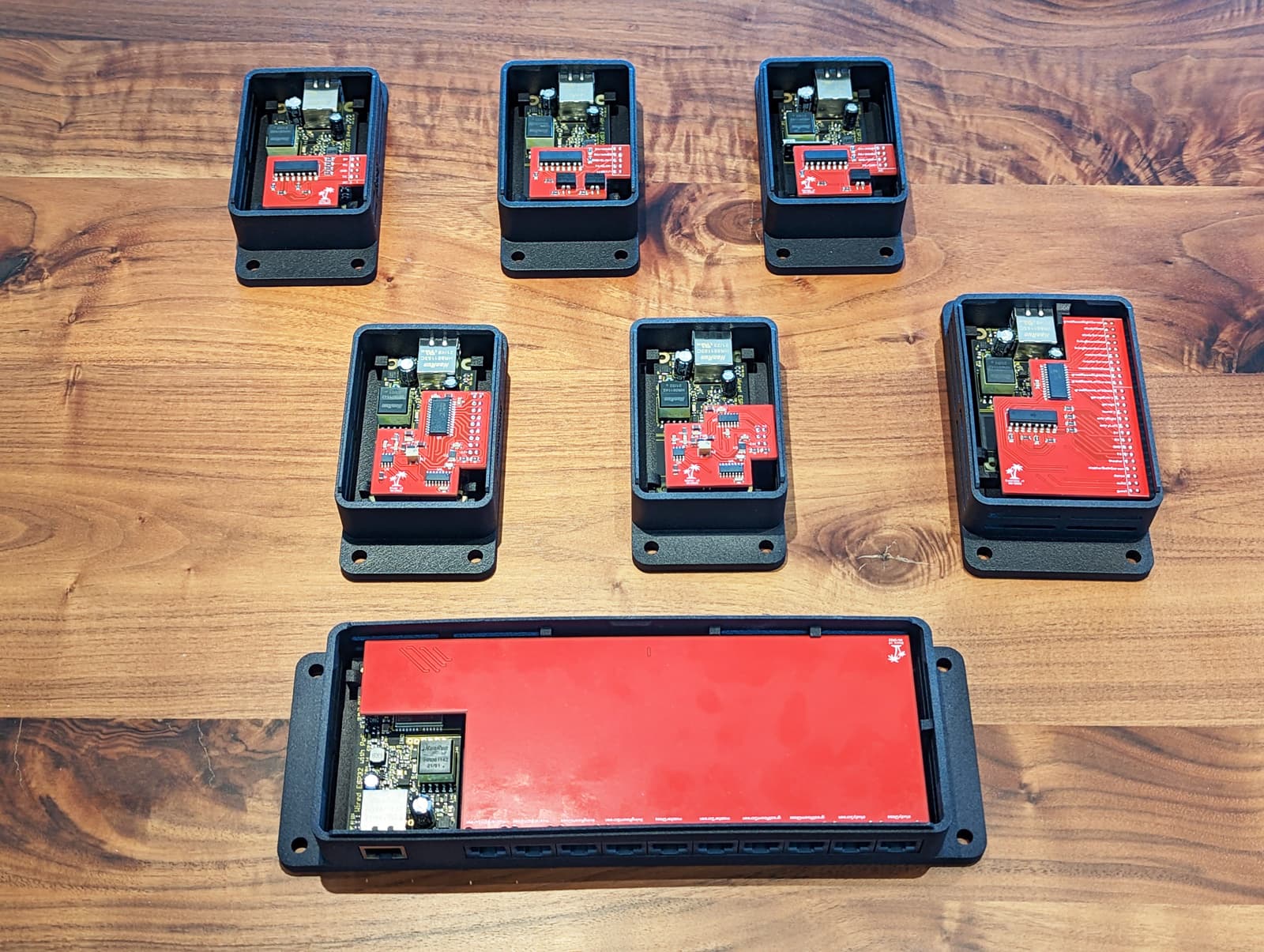
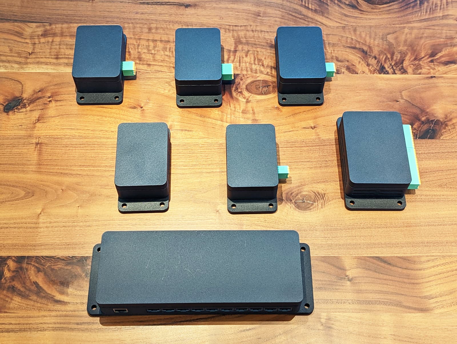
I've also made a number of other boxes for various home automation tasks:
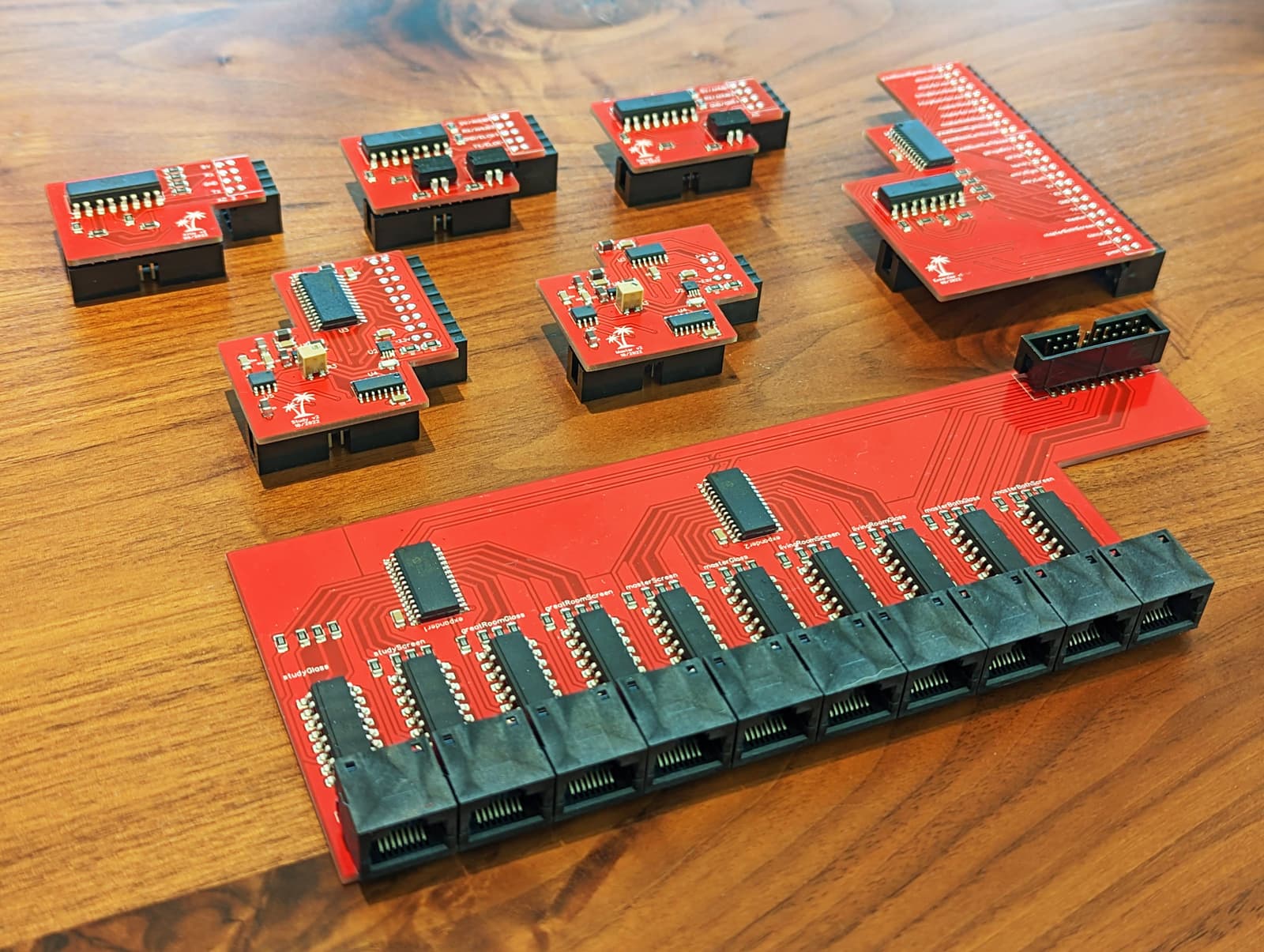
Those control:

  • 10 motorized sliding doors (open/close/stop/lock via 40 optocouplers)
  • 6 HVAC air handlers (via Swicago with optocouplers for UART isolation)
  • 21 reed door switches (to know when doors are open)
  • Garage door (open/close via SSR)
  • 2 exterior PIN pads (for keyless entry when Unifi Access Hub closes contacts)
  • 2 door motorized door locks (via SSRs)
  • 4 more Tekscan pressure sensors to detect when the master bed is occupied

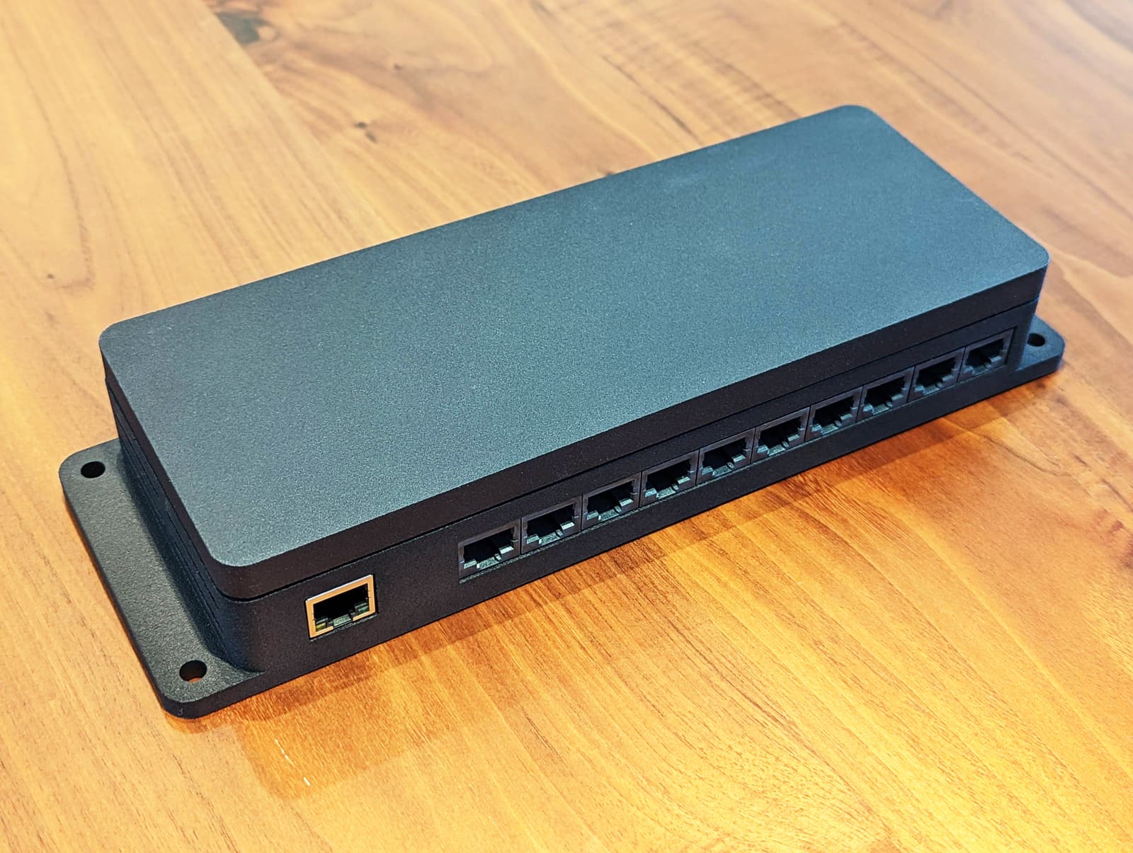
Using SMD is SO much easier than through hole! I wish I had made the switch sooner. If you are stuck doing through stuff, you're doing yourself a serious disservice. Also designing PCBs that don't need any wires is great, specifically the one with 10 ethernet ports. My prototype for that had 70+ wires, it was a nightmare and extremely time consuming to build. Using SMD there's no wires, it's super tidy, and much easier to build.

All this has been a lot of work, but it's quite fun! I'm a bit sad now that I've finished everything, especially since I don't get to play with it yet. I need to come up with new ideas for electronics projects to stay busy until then!

1 Like

That is an amazing and professional looking job. Kudos!
You're right, that enclosure doesn't look 3D printed at all.

Kudos, too for a. just making a followup and, b. doing a bang up job of it.

Great job, all of it! Your knowledge has grown exponentially as you developed this, that shows. The feedback is great. You need to give yourself a pat on the back. Have a drink of your favorite beverage for us:-)

Really nice job!

Well done :smile:

Wow! That all looks great! And I can't wait to see the stairs in action. Thanks for the follow-up, and thanks for pinging me, as I wouldn't have seen your post otherwise.

BTW, I'm curious about the two places where you have a large-ish value capacitor (10 uF or 4.7 uF) in series with a 0.1 uF. What's the rationale for that? I expect them to be in parallel.

image

image

Thanks everybody!

@DaveEvans ah crap, that's a bungle. I couldn't have been thinking there. What I have gives 1/(1/0.1+1/10)=0.099uF, so basically the larger capacitor does nothing. Do you think the mistake is significant? To fix it properly I'd need to order a new board and solder everything again. Two boards actually, as I made the same mistake for the bed force sensors PCB.

The goal was to smooth out any low frequency voltage dips. For the charge pump and mux, I added a 10uF "just in case". For the ADC, the datasheet showed the 4.7uF (wired properly!). I do still have 10uF where +3.3V comes into my PCB, so it seems that should just about do the same job, if a little slower than 4.7uF.

Hmmm...

Not only are the larger capacitors not doing their job, my guess is that the 0.1uF capacitors are less effective due to the additional ESR of the larger capacitors.

But my approach would be to try it as-is and see what happens. :slight_smile:

OK, thanks. It works in my testing, so I'll keep it in mind if I run into any issues.

Here's the current state of the stairs:

16 wires for LED strips, 16 wires for sensors.

1 Like

I suggest you replace the large value series capacitors with wire links. They are not doing anything useful and are probably degrading the performance of the smaller ones they are in series with.

1 Like

Thanks. I had trouble getting to sleep last night and had the same thought. I'll replace the 10uF with 0ohm jumpers.

BTW: nice soldering equipment!

Thanks! It's unnecessary, but it's super nice to use.

What do you guys think of replacing the larger decoupling capacitor with a jumper, then stacking the larger capacitor on top of the 0.1uF? That seems like a reasonable way to achieve the original intention without remaking the whole board, as long as there aren't any proximity issues (heat, vibration, or something else).

No problem with that.

Not my proudest work, but it is done. Behold, capacitor piggybacks:

Oops, didn't notice the IPA left some residue. Better than flux I suppose.

1 Like

If it makes you feel better, I've seen the same thing done on a $3million+ project :slight_smile:

New/late to this string but I’ll echo all the compliments!! Very impressive!! Have you already posted about your SMT equipment? I have built a couple small projects using through hole and it is a massive pain. All info would be appreciated
Again, congrats!!

Thanks!

The JBC soldering iron is really amazing. The heating element is very close to the tip so it heats up near instantly and the tips are great. Stupidly expensive though. The hotplate is nice, though I think having only a hot air tool would be sufficient. Technically you aren't supposed to use only the hotplate to melt solder and I always hit it with hot air at the same time. The JBC hot air tool is nice, but it's quite simple and probably cheaper brands are just as nice. Unique to JBC is their desoldering cups and "spiders" that pull an IC straight up using suction, so as soon as the hot air melts the solder, it lifts it. I've used those a couple times and they are neat.

Definitely making the move from through hole to PCB and hot air tool should be done early. It's sooo much easier, cleaner, and the results are better, very professional. It requires learning some software (DipTrace), using a service like JLCPCB, and getting a hot air tool. Totally worth it. You can easily get by with a cheap soldering iron for the little through hole soldering needed for connectors and such.

Update on the stairs: sadly there is no update. The house is going to be amazing, but it's taking ages. It could take until December 2023. :frowning:

A little update, cladding on the stairs and tidy wiring:

There's 16 cables to force sensors on one side and 16 cables to LED strips on the other side, for individual control. It will still be quite some time until it's functional.

In other news I've gotten better at electronics in general, though still a noob. I've started a bunch of little projects, being careful not to finish any of them. It's that New Relationship Energy, just can't get enough. The most complex project has microphones and a speaker using I2S and an amp, a bunch of LEDs, and air quality sensors. I'm using 6 layer boards and a fancy Xmos IC. Another cool project is using an AFBR-S50 lidar sensor. For that I had to figure out how to use an STM32 (dev board anyway).

Also I've got a reflow oven now, a Controleo3. It works great! Stepping up from hot air to an oven feels similar in magnitude to the step from an iron to hot air. An iron and hot air still have their place, but SMT is sooo much easier now. I got the oven after ruining 5-6 ICs using hot air where all the pins are completely underneath.

1 Like

This topic was automatically closed 180 days after the last reply. New replies are no longer allowed.