Hi, can anybody tell me what use have the solder pads near D7 and D8 Pin on the back side of the board?
Do you mean these ?
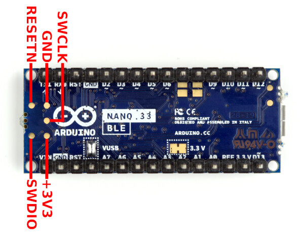
They are used for programming with an external programmer
Hi, no I mean the pins at D7 and D8 in your image in the upper pin row at the place "D7" and "D8".
It looks like a solder bridge that can be bridged but for what use?

Regardless of any particular purpose for the user, its not unknown for PCB manufacturers to put pads on PCBs to make testing or programming of manufactured boards easier. Do a Google search on 'pogo pins'
That there are pads does not imply that you should be soldering stuff to them.
But why the question ?
Hello @oqibidipo , that was exactely what I was looking for.
Many Thanks.
Hello @srnet ,
it is obvious that those pins are not incircuit test pins but pins to make solder bridges by the user. They have different form and size, maybe you should google that or spare such comments please.
@lowenergy , I have to disagree. Any exposed pad can be used for any purpose. Sometimes it's a solder bridge, sometimes it's a test point and sometimes it's for the user to solder to to enable additional functionality. Sometimes it all of the above.
Its 40 years since I first designed a PCB for production.
Since then I have seen a number of test pads like that, often smaller, but sometimes that size too. They are used on vacuum jigs etc. Google 'Genrad ATE' for some examples.
The pads are labelled a Serial Wire Debug interface.
The pads are also spaced on a 0.1" matrix relative to the mount holes so ideally placed for making a push on debug adapter with pogo pins. Sparkfun make one for instance.
This topic was automatically closed 180 days after the last reply. New replies are no longer allowed.