CD4014 (BE) - Understanding the truth table

greets

I've got a CD4014BE shift register that I want to use with 8 switches. I've found some code online but unfortunately it is not helpful for understanding how the shift register works.

So I decided to build a simple circuit with switches connected to the Serial Load, Paralel/Serial Enable and the Clock pins, and to the input pins. Basically I'm duplicating what a MCU does but at very slow speed.

I did this before with a 74HC164 shift register and it clarified for me how it functions, but with the CD4014 it's a different story.

Data Sheet for the CD4014: http://www.unisonic.com.tw/datasheet/CD4014B.pdf

The schematic of my breadboard circuit (see attach): (the pull-down resistors, debouncing caps and current limiting resistors are omitted on the image but present in the circuit).

Here's how I use the switches to duplicate what the MCU does:

(the Serial Input is LOW at all times, I'm not daisy chaining (yet)).

  1. PE (parallel enable - pin 9) - HIGH
  2. Input(s) n - HIGH ( I did this with one of the 8 inputs and in another test with two inputs simultaneously)
  3. CLK - HIGH then LOW (this is CLK pulse #1)
  4. Input(s) n - LOW
  5. PE - LOW
  6. CLK - HIGH then LOW (CLK pulse #2)
  7. CLK - HIGH then LOW (CLK pulse #3)
  8. CLK - HIGH then LOW (CLK pulse #4)
  9. CLK - HIGH then LOW (CLK pulse #5)
  10. CLK - HIGH then LOW (CLK pulse #6)
  11. CLK - HIGH then LOW (CLK pulse #7)
  12. CLK - HIGH then LOW (CLK pulse #8)

then repeat the same steps again over and over. While doing the tests I wrote down the output state of Q8.

I'm not sure if this is the correct way to do it but I got some results that I don't understand.

According to the output table (image CD4014 - Q8 output.jpg) setting input 1 or 2 or 3 HIGH yields the same result at Q8, i.e. :

CLK#1 - 0
CLK#2 - 0
CLK#3 - 0
CLK#4 - 0
CLK#5 - 0
CLK#6 - 1
CLK#7 - 0
CLK#8 - 0

also the combination of Inputs 1+3 HIGH is the same as Input 1 HIGH,
also Inputs 2+4 is the same as Input 4, and so on....

I don't now if my method is correct but if it is, how does the MCU know whether it was input 1, 2 or 3 that went HIGH?

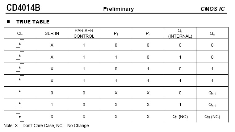
What does Q1(Internal) mean?

What does Qn-1 do?

thanks in advance

p.s. I've just updated the schematic image. The first one was wrong, the 8 input switches should be connected to VDD, not ground.

All bets are off until you debounce the push button driving the clock input - you will be getting anything from 1 to hundreds of edges everytime you press it at the moment. Mechanical
switches should never drive logic clocks directly for this reason!

MarkT:
All bets are off until you debounce the push button driving the clock input - you will be getting anything from 1 to hundreds of edges everytime you press it at the moment.

I did debounce the switches with capacitors (they're just not pictured in the image).

I read the truth table simply. Here is it in English.

The truth table says that when the PAR/SER CONTROL pin is held high and the clock rises, the 8 bits present on the 8 preset pins are transferred into the 8 internal flip-flops. Under these conditions, the chip does not advance these 8 bits at all and SER IN is completely ignored. This is called a "preset" function.

When the PAR/SER CONTROL pin is held low and the clock rises, it acts as a serial shift register. SER IN is placed into Q1, Q1 goes into Q2 ... Q7 goes into Q8.

In either case, after the clock rises, Q6, Q7, and Q8 are available on their respective output pins.

Clock falling doesn't do a thing, as you would expect.

Is this not happening? Have you hit all pins with a logic probe to make sure they have the voltage you think they do?

That is what the data sheet says, at least. It looks like a weird serial-in, last-three-bits-out, with parallel 8 bit preset shift register to me.

Have you hit all pins with a logic probe to make sure they have the voltage you think they do?

thanks for the advice! I went and checked the switches and some of them were faulty. Gonna replace them and do the tests again.

naut:

Have you hit all pins with a logic probe to make sure they have the voltage you think they do?

thanks for the advice! I went and checked the switches and some of them were faulty. Gonna replace them and do the tests again.

Sometimes it's the simple things.

I have been having trouble with a new microcontroller that I have been trying to get working. It's from a different manufacturer, has a different programming environment and different programmer than Atmel. I could get a simple program to compile but the programmer would fail to connect. I thought it was some lapse in my understanding of the S12XE architecture or pin assignments that was causing problems, or maybe the Codewarrior environment, or the (weird) P&E programmer. Nope, I got that all right. There was one very important pin that was left unsoldered accidentally (TQFP package - small pins!) and I finally found it by continuity testing every single connection on the board and then every single pin on my adapter. It was a much simpler error than I thought it was going to be. I actually had the board right, all except for that pin. Now it all works perfectly.

p.s. I've just updated the schematic image. The first one was wrong, the 8 input switches should be connected to VDD, not ground.

You better do it again because that is wrong as well.
You need the switch between input and ground then you need a pull up resistor from each input to 5V. A value between 1K and 10K will be fine.

You need the switch between input and ground then you need a pull up resistor from each input to 5V. A value between 1K and 10K will be fine.

Why? I've used pull-down resistors (they're just not on the picture), everything works fine.

naut:

You need the switch between input and ground then you need a pull up resistor from each input to 5V. A value between 1K and 10K will be fine.

Why? I've used pull-down resistors (they're just not on the picture), everything works fine.

Many people are missing your original caveat. Maybe if it was on the image itself it wouldn't get overlooked (include values):

naut:
The schematic of my breadboard circuit (see attach): (the pull-down resistors, debouncing caps and current limiting resistors are omitted on the image but present in the circuit).

naut:

MarkT:
All bets are off until you debounce the push button driving the clock input - you will be getting anything from 1 to hundreds of edges everytime you press it at the moment.

I did debounce the switches with capacitors (they're just not pictured in the image).

That only works if you pass the signal through a schmidt-trigger gate. All bets are off
until you properly debounce that clock signal.

[ feeding a slowly varying signal to a logic input that isn't a schmidt-trigger may cause
various issues, multiple edges, oscillation, increased power consumption (shoot-through)
and in worst cases illegal internal states. Often this is overlooked and the results aren't
even noticed, but for a clock signal its often a show-stopper like this.

For logic gates the band of voltages between VIH and VIL is termed the forbidden zone,
and for correct circuit operation signals are expected to pass through that zone in a few
tens to hundreds of nanoseconds depending on the logic family. The 4000 series is slow
so a microsecond or so is probably OK, but that's still 5 million volts per second...

A schmidt-trigger gate uses positive feedback to turn a slowly changing input into a full-speed
transition on the output. ]

I've used pull-down resistors (they're just not on the picture), everything works fine.

Fantastic. The only snag is that sadly I am not a mind reader.

I know you said that:-

(the pull-down resistors, debouncing caps and current limiting resistors are omitted on the image but present in the circuit).

But you then went on to say you had changed the circuit. How can you expect good help if you are not willing to make the effort to show what you have? For all we know you put those parts in wrong, a lot of people asking for help do.

Read the how to use the forum sticky, it says their not to change things on the initial post.

Grumpy_Mike:
Read the how to use the forum sticky, it says their not to change things on the initial post.

Sorry about that.

I updated the schematic (see attach).

That only works if you pass the signal through a schmidt-trigger gate. All bets are off
until you properly debounce that clock signal.

Yep, true, but I decided not to use a schmidt-trigger gate just to see what happens, it worked, probably because I press the buttons and hold them for ca. half a second before releasing, I even removed the caps and was it ok (of course normally I would not omit a proper debouncing circuit).

feeding a slowly varying signal to a logic input that isn't a schmidt-trigger may cause
various issues, multiple edges, oscillation, increased power consumption (shoot-through)
and in worst cases illegal internal states.

So it's not realistic to use capacitors with a capacitance value that will be large enough to debounce the switch but small enough enough as to not to cause a slow varying signal?

naut:
So it's not realistic to use capacitors with a capacitance value that will be large enough to debounce the switch but small enough enough as to not to cause a slow varying signal?

No, since debouncing is in the realm of several milliseconds, slow transitions are in realm
of a few microseconds for fast logic families (and very noise dependent).

Try R1 = 1k, R2 = 10k, C = 10uF. The gate can be a 74HC14 hex schmitt inverter.

You can also drive the clock input from an Arduino pin of course.

I fear I mis-spelled schmitt before, BTW. In my defence I note that Wikipedia uses
both spellings in their article (checkout the first image on the RHS)

This discussion is all for TTL/CMOS, though, and not AVR, right? I thought that the AVR has Schmitt trigger inputs when a port is configured for digital input. Is that right?

JoeN:
This discussion is all for TTL/CMOS, though, and not AVR, right? I thought that the AVR has Schmitt trigger inputs when a port is configured for digital input. Is that right?

Yes, the ATmega family have about 10% hysteresis, according to the datasheets. Not enough
for very noisy environments perhaps, but enough to prevent the common problems. 74HC14
has about 20% hysteresis (typical).