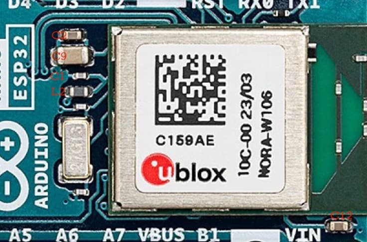
I am wondering if perhaps someobody could shed some light on the reason behind the order of decoupling capacitors in the Arduino Nano ESP32 power rails,
The VCC pin contains first the bulk decoupling capacitor 10uF to ensure a stable voltage and filter low-frequency noise followed by a smaller, high-frequency filtering cap of 100nF. The latter is always placed as close as possible to the MCU pin to shunt the switching noise to GND.
On the other hand, on the VCCIO rail we have a bit more filtering to get cleaner IO signals. So they put a LC filter followed by a bulk decoupling cap that is now a bit smaller i.e. 1uF. While I understand that the LC filter might have been tuned to circuit, what I don't understand is why there is no 100nF decoupling cap after the 1uF cap. Is it because they decided to merge the 10uF and 100nF into a single cap that's inbetween to reduce the number of components?
Or did they expect the LC filter to already be so good at filtering out the high frequency noise that they decided to skip the 100nF cap?
Alternatively, wouldn't it have been better to first put the bulk decoupling capacitor and then create a pi filter instead (100nF + 2nH + 100nF)?
Also, isn't it good practice to have at leat one 100nF decoupling cap for each pin, here we have two VCCIO and one VDD_SPI pin. Is the LC filter really the solution here?
Thanks for your reply. Yes I read the datasheet and integration manual for NORA W106 and unfortunately they do not offer any guidance on the power supply side and assume standard practice. There is an EVK-NORA-W10 demo board which has quite different power rail choices as compared to the Arduino Nano esp32 version.
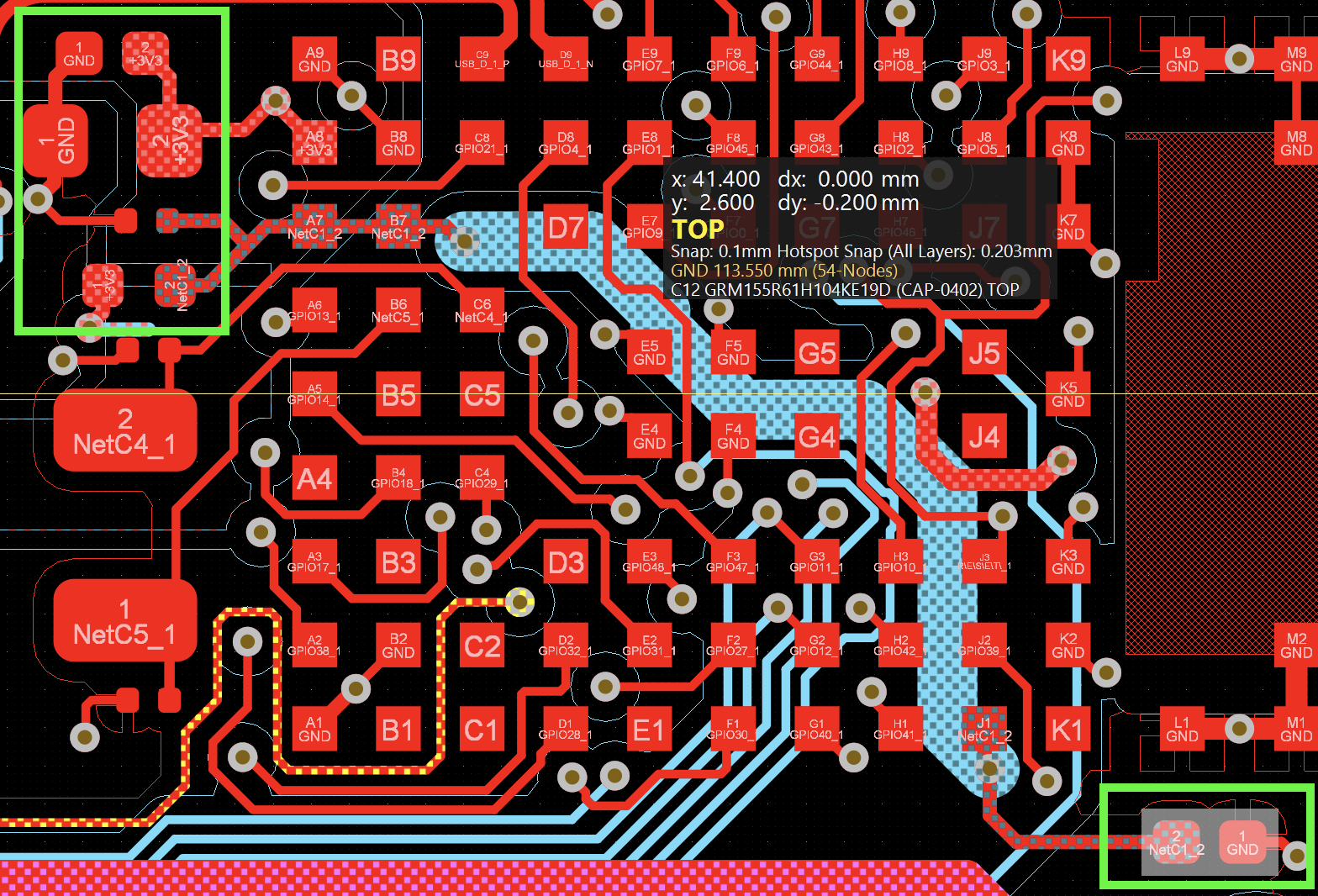
It appears that the C12 100nF capacitor is deliberately placed near the VDD_SPI pin (which is on the other side), whil L2+C1 are placed near the VCCIO pins, so in this case it seems that whoever designed this believed that an LC filter can in this case both supress high+low frequency noise and provide votlage stability at the same time.
Now upon closer inspection I noticed that C9 is actually placed closer to the VCC pin (unlike in the schematic) while the 100nF C2 cap is connected in parallel to it, again an unconventional choice but in this case I don't think it matters since both are very close to the VCC pin.
Now looking at the PCB I can see even more strange choices, such as the filtered VCCIO rail being a nice thick trace on the bottom layer (indicated in cyan), but when they connect the 3.3V rail to the pins they use thin traces which are suitable for signals but seems like a strange choice for a power rail, especially given there is quite enough space for a thick trace here.
Maybe because putting a second 100nF capacitor together with the bulk capacitor now is considered a bit old school. Maybe in the past with THD components, the smaller capacitor had less inductance. But today with SMD multilayer capacitors it is not necessary.
Two capacitors can perform better, but doesn't need to be smaller.
Anyway, better stick to the datasheet of the component. Capacitors are cheap and small.
And if you want to put two for redundancy or better ESR, put both capacitors of 1uF, or both 22uF...