I am using ESP8266 on my PCB prototype. I have some doubts about what should I pay attention to for RF immunity of ESP8266. For example, Should the ground plane lay down under right below of antenna or not?
Except then this, I have paid attention to place esp8266 away from other noise generators such as oscillators, switching voltage regulators and other RF modules. And, I have supplied power to the chip sufficiently with strong regulator and required capacitors. Moreover, I have placed many vias where it supposed to be.
What do you think about what can be done more for improvement?
wvmarle:
NO copper whatsoever under the antenna. If possible, let the antenna protrude out of the board.
Make sure the 100nF and 100 uF decoupling caps are placed close to the Vcc pin.
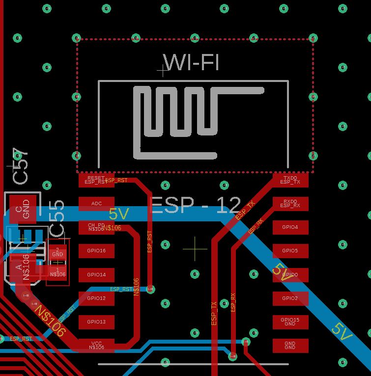
Thank Mvmarle for your response, since all edges of my PCB are fulfilled with other components and connectors, it seems it is not possible to keep antenna out of the board for now. However, it will be so definitely for the next version. To save today, how big should the "NO copper" area be? Is quite bigger than the antenna section of the module like below screenshots?
Same size as the antenna.
That's at least what the KiCAD footprint of the part tells me to do.
BlindWolf:
ince all edges of my PCB are fulfilled with other components and connectors, it seems it is not possible to keep antenna out of the board for now. However, it will be so definitely for the next version.
wvmarle:
Same size as the antenna.
That's at least what the KiCAD footprint of the part tells me to do.
I thought you're currently designing that board??
Yes, I am currently in the process of design. What I meant there is the case of PCB and other external tools are designed and ordered so. Therefore I cannot get the antenna out of the board for this version.
BlindWolf:
Yes, I am currently in the process of design. What I meant there is the case of PCB and other external tools are designed and ordered so. Therefore I cannot get the antenna out of the board for this version.
Then be prepared for less than reliable operation.
Or swap it out for an ESP-7S module, they're a bit smaller and have a connection for external antenna. Connections to the PCB I remember are identical to the ESP-12 module. Then the antenna can be bigger and away from the PCB itself. Note that the ESP-7 (with also some kind of on board antenna) has less flash memory.
I've myself done boards with the ESP-12 in the middle, it does work quite well, but you definitely have to keep all copper away from under the antenna, that accounts for all layers of the board.
wvmarle:
Or swap it out for an ESP-7S module, they're a bit smaller and have a connection for external antenna. Connections to the PCB I remember are identical to the ESP-12 module. Then the antenna can be bigger and away from the PCB itself. Note that the ESP-7 (with also some kind of on board antenna) has less flash memory.
I've myself done boards with the ESP-12 in the middle, it does work quite well, but you definitely have to keep all copper away from under the antenna, that accounts for all layers of the board.
Esp7 seems like the best solution for now. Even I am not using its flash memory a lot. However, as productivity get higher through the end, I come up with a brilliant solution. How about even drilling/ milling the bottom of the antenna instead of not just "no copper area"? (I know it is still not better then placing the module on the edge)
I see that the copper layer bottom of the antenna behaves like an RF shield. I wonder How the naked FR4 PCB reacts for RF waves?
If you are struggling to avoid copper close to the antenna then one option is to extend the pins so the boards are far apart. I have ESP8266s on breadboard with a gap of over 15mm, they work fine. They didn't work when they were plugged directly into the breadboard.
In your next rev, consider using an ESP-01M - takes up way less board space because it gets inserted at 90-degree angle and soldered in place, which also gets the antenna up away from the board a bit.
It seems to me that the OP uses an ESP12 which is much more capable as it has all GPIO available. I'm using those modules to run rather complex projects.
DrAzzy:
In your next rev, consider using an ESP-01M - takes up way less board space because it gets inserted at 90-degree angle and soldered in place, which also gets the antenna up away from the board a bit.
I did not know such a module. esp01 vertical placing can be a good solution for both signal and space problems. Thank you DrAzzy.
[/quote]
Paul__B:
You are suggesting fouling up the antenna? That is what it sounds like. The antenna is properly designed. It is not the problem.
The problem is that you must not place copper areas - and preferably not much bare PCB either - anywhere near the antenna.
No no, I am talking about cutting out the area where the antenna of the module is placed on my PCB(like the attached image below), not the bottom of the module. What I wonder is just whether there is a change in performance and signal quality of ESP between methods in the attached two images or not. (?) .
To be more specific, How does FR4 without copper on both side behave as a medium for RF waves? Does it let pass all signals without any loss? I think of course it is much better to pass signals than copper. If air and FR4 without copper on both sides are compared, do you think the reasonable difference is got between them?