Hi! I have made a PCB schematic for my project that I was talking about in this post Project ideea and approach
The schematic represents the TX unit of my project, which is powered by a 3.7v 300mAh LiPo battery, with the press of the button a code is transmitted to the RX unit that will be the same except it will be programmed accordingly and it will control a 3.7v servo. I hope everything is okay, I mostly mean the Ra 02 wiring and the extra capacitors for it, the voltage converter should be ok, I will attach a datasheet for it, basically I followed the typical application schematic for it, and I will add a pad for the UPDI programming. Is everything okay? Thank you in advance!
LED 1 and LED 2 should have a resistor each, especially if they will be lit at the same time and especially if they are different colours. 68Ohms seems too low. Rule of thumb 220Ohms. How did you calculate the value?
For the power consumption maybe you could check if an LDO would be more efficient than the buck, in this case, because of the very low current.
I understand that the device will be activated once every 20/30 minutes, so it will be sleeping almost all the time, consuming a few µA. Make sure that both the MCU and the RA-02 are put to sleep between activations.
The Attiny power consumption in sleep mode is about 2µA, and the RA-02 is around 1µA, if I'm not wrong.
For that small currents could be that a low power LDO is more efficient than a switching regulator.
Even if it's similar, you wouldn't need the inductor in the PCB. And the output voltage will be more clean.
You could test it, while sleeping the total current consumption should be about 10 or 20 µA.
You could also consider a regulator of 3.0V output instead of 3.3V. This way you use a bit more of the battery capacity. Both devices can work fine at 3V or less.
Anyway could be that the 3.3V buck/LDO, continue working below 3.3V just following the voltage down. You should test it.
The leds won't work at the same time, if LoRa doesn't initialize correctly then the Led2(Red) will be lit to show that there is an error and the code with be stuck/paused, when everything is normal Led1 will blink when the button is pressed, the leds have a voltage rating of 2.8v I think, so from 3.3v and the resistor that should be good I guess?
Is a ground plane necessary? All the GNDs are connected together. Wider tracks means more space... if the LoRa consumes about 100mA working as a TX are the 0.254mm traces going to work?
OK, probably OK then. My preference would still be 2 resistors because doing so means you are free to change your code to have both lit at the same time should you decide to do so.
Both red? Or different colours? Different colours have different Vf. 2.8V for red seems to be too high, more typical would be 1.6V to 2V I think. See:
Based on 2.8V and 3.3V supply:
3.3 - 2.8 = 0.5
0.5 / 68 = 7.3mA, which I guess is OK. It just looked too low to me.
There's plenty of room on that PCB for wider tracks, especially the power. The back is hardly used.
Good question, and I am not experienced enough in PCB design to give you a clear 'you must have' or 'it doesn't matter' response, but it seems daft to me not to fill the back with copper connected to ground. At least in part that is what ground is, as well as being 0V. To me it is in the same category as decoupling capacitors: maybe your circuit will work OK without them, but it makes no sense to leave them out so you put them in. Same with ground plane, just include it. Maybe someone else will give you a clearer answer.
No, but it won't hurt either. I generally route power on one side (usually bottom) and signal on the other side (usually top), making exceptions where necessary. As @PerryBebbington says, you're presently not using the bottom side, and for a one-off or small volume PCB there's hardly any penalty cost-wise for making a double-sided PCB. Also, as he mentions, you're paying for the copper, so might as well leave it on there - i.e. use wider traces for power.
Not sure why the single resistor for both LEDs is needed; resistors this size are virtually free. Just thrown in an extra one. If you're short on space, replace the LEDs with SMD ones, which will make the whole thing a little more compact.
Other than that, looking good; I'm sure you'll get there.
Yes, but it looks to me this LoRa module uses an external antenna. These generally connect with the board with a small coax cable, so having a ground pour near that connection on the module won't make a difference, since the antenna cable is shielded anyway. However, if you meant "don't hide the actual antenna behind a PCB ground plane", then yes, absolutely. It will affect range.
I missed that, I've never used LoRa, so I am not familiar with the boards. Agreed, if the antenna is external there's no need to leave off the ground pour anywhere, just over the whole back of the board, except for where there are non-ground tracks.
The problem here is the space as it will be with all my projects, I make PCBs that are going to be placed on free flight model gliders so the other side of the PCB will be exposed and should not have any pads and SMD modules to prevent short-circuits. I wanted to use 0906 format of SMD resistors, capacitors, etc. But they are to small to be soldered by hand. But I will try to adjust this PCB, that will be used as a TX remote, because here the space doesn't matter too much. I will replace the 5mm LEDs with 3mm LEDs, they are supposed to peek trough a lid of a box so I can't use SMD ones. What width should I use for the copper traces? Also how do I program the Attiny trough UPDI, I mean what resistors and components do I need, I keep seeing different resistor values, 4.7k or 10k..can I program it with an ISP programmer or a TTL one?
Is there some reason you're avoiding traces on the bottom of the board?
I don't like traces between SMT pins, and the trace between the two end upper pins on the lora module is (needlessly) close to the other pads.
There are certainly smaller SW2 and LEDs. Have you thought about putting u1 on the other side of the board?
Your vias look very tiny; do they actually work WRT your board maker?
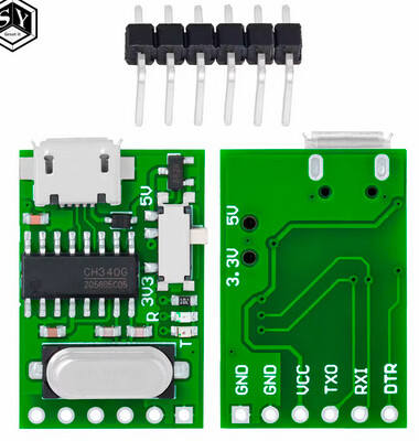
You just need a normal USB serial adapter, a diode and a 470Ω resistor.
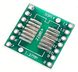
And first of all, I would strongly recommend to put one Attiny MCU in a SOP adapter and mount it in a breadboard:
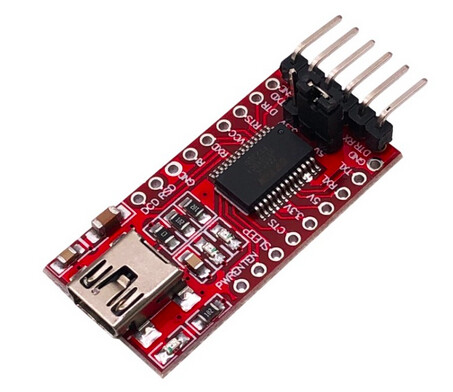
For the programmer, this one works very well and is very cheap:
But anyone that you already have should also work, like this one:
Better put the adapter, the diode and the resistor in a separated small breadboard.
This will work. Make sure that you can program the MCU alone with a blinky led. And then build the rest, before ordering the PCB.
I would also recommend to add another wire to be able to debug with Serial.println(), but you have to add a switch because it uses the same RX-TX line. It's almost the same:
To program open the switch and to debug close the switch.
Instead of the switch you can just move the dupont jump from one place to the other, but the switch is much better. Specially when you realize that you have to do it about 1000 times.
0906 is uncommon. 0805 is a close size that's very common, and in my opinion, 0805 is really easy to hand solder. The same goes for 0603. Things get iffy at 0402 and smaller, although that size still hand solders OK with a little bit of care. I think you just need to practice a little if you're having trouble hand soldering 0805; there's really nothing particularly troublesome about it.
OK, I can see what you mean, although I'd counter this by suggesting to use a simple light guide.
It's not very critical. I'd go with >1.5mm for the power traces. Nothing on this circuit is particularly power-hungry, so this is mostly about reducing noise during rapid transients.
You only need an UPDI line and power + GND on your target board. Nothing else. It's really simple.
To make an UPDI programmer from a USB-UART bridge, I use this arrangement:
UART RX and TX on the left, UPDI on the right. The resistor is 1k, the diode is a generic Schottky. The TX and RX in this case are on a CH340, but I assume it'll work just as well with a CP210x, FTDI232 etc. You could of course also put this arrangement on the target board so you can plug in any old USB-UART device.
UPDI is in-system programming (ISP). It does not use SPI evidently and I'm not sure you can program these devices with SPI like you do with the old-style ATtiny's and ATmega's.
Not sure what you mean with TTL; maybe USB-UART?
Anyway, UPDI works perfectly fine and is very convenient, so I wouldn't bother with anything else. You can use UART for Serial monitor debugging of course.
and place it on a breadboard with other components, but I could also solder in on the PCB and leave the UPDI pad and then program it while soldered on the PCB. What solution would be better?
I was wrong here I wanted to use and purchased 0603 format SMD capacitors and I tried to solder one, and it's not that hard, although I would need a microscope or something.
What distance should I have in mm between cooper tracks and or pads? Let's just say for 150mA and 3.3v?
Whichever you prefer. I just include a single-row pin header on the project PCB that has power and UPDI for programming, that's all.
I find that I can still do it with the naked eye, but use a loupe to verify the solder joints when I'm done. A microscope is nice, but you can also use a loupe on a stand or something. Something like this:
I generally use 0.2mm, which is already way more than enough to prevent problems. 3.3V and 5V don't travel very far on FR4 PCB material. It's different if you're going to work with higher voltages (>100V).