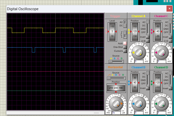
I am trying to create a 3 phase sine PWM signal from all 6 pins using the code from https://github.com/cmasenas/3-Phase-Sine-Arduino/blob/Release/DDS_Generator.ino Modified to be 6 pins (with low side) which can be used OCR1A (High A) and OCR1B (Low A or Inverting Mode of OCR1A), OCR4A (High B) and OCR4B (Low B), OCR3A (High C) and OCR3B (Low C). After trying to simulate in the program, it was found that phase A has no problem, phase C has no problem. But phase B (OCR4B cannot be invert of OCR4A) has a problem. Please help me view and edit the code.Use code tags to format code for the forum
#include "avr/pgmspace.h"
/*#define Nsample 256
#define Nsample_2_3 175
#define Nsample_1_3 85*/
//#include "PWM2560EBIKE.h"

// Look Up table of a single sine period divied up into 256 values.
const PROGMEM int sine256[]  = {
  127,130,133,136,139,143,146,149,152,155,158,161,164,167,170,173,176,178,181,184,187,190,192,195,198,200,203,205,208,210,212,215,217,219,221,223,225,227,229,231,233,234,236,238,239,240,
  242,243,244,245,247,248,249,249,250,251,252,252,253,253,253,254,254,254,254,254,254,254,253,253,253,252,252,251,250,249,249,248,247,245,244,243,242,240,239,238,236,234,233,231,229,227,225,223,
  221,219,217,215,212,210,208,205,203,200,198,195,192,190,187,184,181,178,176,173,170,167,164,161,158,155,152,149,146,143,139,136,133,130,127,124,121,118,115,111,108,105,102,99,96,93,90,87,84,81,78,
  76,73,70,67,64,62,59,56,54,51,49,46,44,42,39,37,35,33,31,29,27,25,23,21,20,18,16,15,14,12,11,10,9,7,6,5,5,4,3,2,2,1,1,1,0,0,0,0,0,0,0,1,1,1,2,2,3,4,5,5,6,7,9,10,11,12,14,15,16,18,20,21,23,25,27,29,31,
  33,35,37,39,42,44,46,49,51,54,56,59,62,64,67,70,73,76,78,81,84,87,90,93,96,99,102,105,108,111,115,118,121,124
};

/*int Isample_a =0; int Isample_b =0; int Isample_c =0;
int Xsample_a =0; int Xsample_b =0; int Xsample_c =0;
int Vm = 1023;
int Vx = 1023;
int fm = 0;
int Vmid = (ICR1+1)>>1;
int duty = 100;*/

#define cbi(sfr, bit) (_SFR_BYTE(sfr) &= ~_BV(bit)) //define a bit to have the properties of a clear bit operator
#define sbi(sfr, bit) (_SFR_BYTE(sfr) |= _BV(bit)) //define a bit to have the properties of a set bit operator

int deadtime = 2;

//High side
int PWM1 = 11;// PWM1 output, phase 1 OC1A
int PWM2 = 6; //PWM2 ouput, phase 2 OC4B
int PWM3 = 5; //PWM3 output, phase 3 OC3A
//Low side
int PWM4 = 12; //PWM4 output, phase 1 OC1B
int PWM5 = 7; //PWM5 output, phase 2 OC4C
int PWM6 = 2; //PWM5 output, phase 3 OC3B

int phaseshift_1 = 85; //offset 1 is 120 degrees out of phase 256/3 = 85
int phaseshift_2 = 170; //offset 2 is 120 degrees out of phase 256*2/3 = 170

double dfreq;
const double refclk=31376.6;      // measured output switching frequency

// variables used inside interrupt service declared as voilatile
volatile byte current_count;              // Keep track of where the current count is in sine 256 array
volatile byte ms4_delay;             //variable used to generate a 4ms delay
volatile byte c4ms;              // after every 4ms this variable is incremented, its used to create a delay of 1 second
volatile unsigned long phase_accumulator;
volatile unsigned long tword_m;  // dds tuning word m
// Hall sensor
/*int HallY = A1;
int HallG = A2;
int HallB = A3;*/

void setup()
{
  pinMode(PWM1, OUTPUT);      //sets the digital pin 11 as output
  pinMode(PWM2, OUTPUT);      //sets the digital pin 6 as output
  pinMode(PWM3, OUTPUT);      //sets the digital pin 5 as output
  pinMode(PWM4, OUTPUT);      //sets the digital pin 12 as output
  pinMode(PWM5, OUTPUT);      //sets the digital pin 7 as output
  pinMode(PWM6, OUTPUT);      //sets the digital pin 2 as output

  Setup_timer1();
  Setup_timer4();
  Setup_timer3();

  //Disable Timer 0 interrupt to avoid any timing delays
  cbi (TIMSK0,TOIE0);              //disable Timer0 delay() is now not available
  sbi (TIMSK1,TOIE1);              //enable Timer2 Interrupt

  dfreq=50.0;                    //initial output frequency = 50.0 Hz
  tword_m=pow(2,32)*dfreq/refclk;  //calulate DDS new tuning word

}
void loop()
{
  while(1)
  {
      if (c4ms > 250) // c4ms = 4ms, thus 4ms *250 = 1 second delay
       {
        c4ms=0;                          //Reset c4ms
        dfreq=analogRead(0);             //Read voltage on analog 0 to see desired output frequency, 0V = 0Hz, 5V = 1.023kHz
        cbi (TIMSK1,TOIE1);              //Disable Timer2 Interrupt
        tword_m=pow(2,32)*dfreq/refclk;  //Calulate DDS new tuning word
        sbi (TIMSK1,TOIE1);              //Enable Timer2 Interrupt

      }
  }
}

void Setup_timer1(void)
{
  // Timer1 Clock Prescaler to : 1
  // Set clock prescale to 1 for maximum PWM frequency
  // TCCR1B |= (0 << CS12) | (0 << CS11) | (1 << CS10); //
  sbi (TCCR1B, CS10);
  cbi (TCCR1B, CS11);
  cbi (TCCR1B, CS12);

  // Timer1 PWM Mode set to Phase Correct PWM มันตั้งได้ 2 Register คือ A กับ B โดยจะตั้ง A เป็น High (Non-invert), B เป็น Low (Invert)
  //      MODE              COMnX1  COMnX2                        DesCription
  // Fast PWM                  1       0        Clear OCnX on compare, Set OCnX at BOTTOM (non-inverting)
  // Fast PWM                  1       1        Set OCnX on compare, Clear OCnX at BOTTOM (inverting)
  // PWM Phase/Freq Correct    1       0        Clear OCnX on compare Up-Cnt, Set OCnX on compare Down-Cnt
  // PWM Phase/Freq Correct    1       1        Set OCnX on compare Up-Cnt, Clear OCnX on compare Down-Cnt

  // TCCR1A |= (1 << COM1A1) | (0 << COM1A0); //non-inverting
  cbi (TCCR1A, COM1A0);
  sbi (TCCR1A, COM1A1);

  // TCCR1A |= (1 << COM1B1) | (1 << COM1B0); //inverting
  sbi (TCCR1A, COM1B0);
  sbi (TCCR1A, COM1B1);

  // Mode 1 / Phase Correct PWM
  sbi (TCCR1A, WGM10);
  cbi (TCCR1A, WGM11);
  cbi (TCCR1B, WGM12);
  cbi (TCCR1B, WGM13);
}

//Timer 1 setup
//Set prscaler to 1, PWM mode to phase correct PWM,  16000000/510 = 31372.55 Hz clock
void Setup_timer4()
{
  // Timer4 Clock Prescaler to : 1
  // TCCR4B |= (0 << CS42) | (0 << CS41) | (1 << CS40);
  sbi (TCCR4B, CS40);
  cbi (TCCR4B, CS41);
  cbi (TCCR4B, CS42);

  // Timer4 PWM Mode set to Phase Correct PWM มันตั้งได้ 2 Register คือ A กับ B โดยจะตั้ง A เป็น High (Non-invert), B เป็น Low (Invert)
  //      MODE              COMnX1  COMnX2                        DesCription
  // Fast PWM                  1       0        Clear OCnX on compare, Set OCnX at BOTTOM (non-inverting)
  // Fast PWM                  1       1        Set OCnX on compare, Clear OCnX at BOTTOM (inverting)
  // PWM Phase/Freq Correct    1       0        Clear OCnX on compare Up-Cnt, Set OCnX on compare Down-Cnt
  // PWM Phase/Freq Correct    1       1        Set OCnX on compare Up-Cnt, Clear OCnX on compare Down-Cnt
  // Timer2 PWM Mode set to Phase Correct PWM

  // TCCR4A |= (1 << COM4A1) | (0 << COM4A0); //non-inverting
  cbi (TCCR4A, COM4A0);  // clear Compare Match
  sbi (TCCR4A, COM4A1);

  // TCCR4A |= (1 << COM4B1) | (1 << COM4B0); //inverting
  sbi (TCCR4A, COM4B0);
  sbi (TCCR4A, COM4B1);

  // Mode 1  / Phase Correct PWM
  sbi (TCCR4A, WGM40);
  cbi (TCCR4A, WGM41);
  cbi (TCCR4B, WGM42);
  cbi (TCCR4B, WGM43);
}

void Setup_timer3()
{
  // Timer3 Clock Prescaler to : 1
  // TCCR3B |= (0 << CS32) | (0 << CS31) | (1 << CS30);
  sbi (TCCR3B, CS30);
  cbi (TCCR3B, CS31);
  cbi (TCCR3B, CS32);

  // Timer3 PWM Mode set to Phase Correct PWM มันตั้งได้ 2 Register คือ A กับ B โดยจะตั้ง A เป็น High (Non-invert), B เป็น Low (Invert)
  //      MODE              COMnX1  COMnX2                        DesCription
  // Fast PWM                  1       0        Clear OCnX on compare, Set OCnX at BOTTOM (non-inverting)
  // Fast PWM                  1       1        Set OCnX on compare, Clear OCnX at BOTTOM (inverting)
  // PWM Phase/Freq Correct    1       0        Clear OCnX on compare Up-Cnt, Set OCnX on compare Down-Cnt
  // PWM Phase/Freq Correct    1       1        Set OCnX on compare Up-Cnt, Clear OCnX on compare Down-Cnt
  // Timer2 PWM Mode set to Phase Correct PWM

  // TCCR3A |= (1 << COM3A1) | (0 << COM3A0); //non-inverting
  cbi (TCCR3A, COM3A0);  // clear Compare Match
  sbi (TCCR3A, COM3A1);

  // TCCR3A |= (1 << COM3B1) | (1 << COM3B0); //inverting
  sbi (TCCR3A, COM3B0);
  sbi (TCCR3A, COM3B1);

  // Mode 1  / Phase Correct PWM
  sbi (TCCR3A, WGM30);
  cbi (TCCR3A, WGM31);
  cbi (TCCR3B, WGM32);
  cbi (TCCR3B, WGM33);
}

//Timer2 Interrupt Service at 31372,550 KHz = 32uSec

//FOUT = (M (REFCLK)) / (2 exp 32)
//Runtime : 8 microseconds
ISR(TIMER1_OVF_vect)
{

  phase_accumulator=phase_accumulator+tword_m; //Adds tuning M word to previoud phase accumulator. refer to DDS_calculator (from Martin Nawrath) for explination.
  current_count=phase_accumulator >> 24;     // use upper 8 bits of phase_accumulator as frequency information

  OCR1A = pgm_read_byte_near(sine256 + current_count); // read value fron ROM sine table and send to PWM
  OCR1B = OCR1A;

  OCR4A = pgm_read_byte_near(sine256 + (uint8_t)(current_count + phaseshift_1)); // read value fron ROM sine table and send to PWM, 120 Degree out of phase of PWM1
  OCR4B = OCR4A;

  OCR3A = pgm_read_byte_near(sine256 + (uint8_t)(current_count + phaseshift_2));// read value fron ROM sine table and send to PWM, 120 Degree out of phase of PWM2
  OCR3B = OCR3A;

  //increment variable ms4_delay every 4mS/125 =  milliseconds 32uS

  if(ms4_delay++ == 125)
  {
    c4ms++;
    ms4_delay=0; //reset count
   }

}
I'm sorry if I did something wrong. Please give me some advice and help. I'm still a beginner.