-
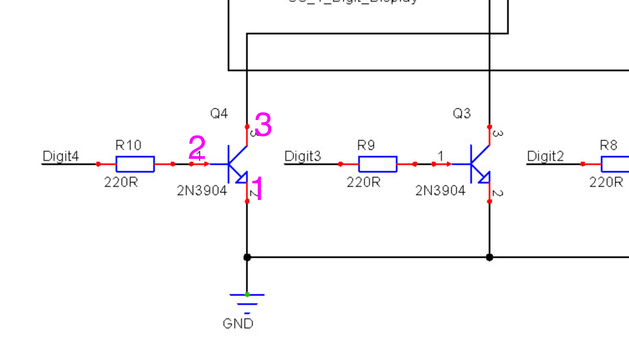
When looking at a schematic, you are responsible to confirm the foot print pin numbers of the transistor which you have.
-
The Base, Emitter and Collector are correctly connected as shown in the schematic.
-
You must always make sure the actual pin numbers agree with your part.
i.e. Your base is pin #2, your Emitter is pin #1 and your Collector is pin #3, design your PCB based on the data sheet for your transistor.

-
Your 2nd image looks suspicious with the base traces, the display footprint looks too small.
-
Always run DRC on the PCB to confirm routing.
-
suggest for just a one of project you use point to point wiring on a prototyping board.

