I would like to get help with ADC due to my limited knowledge.
Currently, I am using 16bit ADC LTC2368-16((https://www.analog.com/media/en/technical-documentation/data-sheets/236816f.pdf),) with Arduino Uno for making measurements at very short intervals, but having problems with noise.
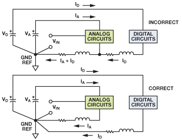
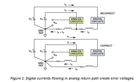
First, let me show the connections to LTC2368 in the figure below, the first attached picture.

Following the datasheet, I set up the device to ‘normal mode, single device’ configuration, with CHAIN and RDL/SDI connected to the GND. When I connected 2.5V reference voltage to IN+ and Vdd and measured the output, peek-to-peek noise was at 50~100LSB (ex. OUTPUT = 10000 ~10050)
At rare moments, the peek-to-peek noise stays very low, below 8LSB, but if I restart Arduino several times or plug the cable at a different port and reconnect, then the noise increases by significant amount, back to 50~100LSB.
Strangely, when I connected 2.5V reference voltage to Adafruit’s ads1115 breakout board (ADS1115 16-Bit ADC - 4 Channel with Programmable Gain Amplifier [STEMMA QT / Qwiic] : ID 1085 : $14.95 : Adafruit Industries, Unique & fun DIY electronics and kits) for comparison and measured the output, peek-to-peek noise was kept at 2LSB, even after a long time.
According to the data sheets, both ADCs have INL of below 1LSB, and while ads1115 has
2.45 times larger input voltage per 1LSB (LTC2368 : 5/2^16, ads1115 : +-6.144/2^16) than ltc2368, LTC2368 has much larger peek to peek noise. Comparing with ads1115, 8LSB seems to be adequate level of noise, but it’s very rare as I’d mentioned above.
I tried connecting additional capacitors following the demoboard example on the datasheet in order to reduce noise but only marginal difference. As shown below, I added 0.1uf and 10uf capacitors to Vdd and OVdd, and 0.1uf and 47uf capacitor to REF PIN in parallel.

What could be the possible cause of large peak-to-peak noise? If I am not understanding something right, which parameter from datasheet should I look into?
Shown below are the Arduino code for measurement and the timing diagram of LTC2368. For Ads 1115, Adafruit’s library was used and the rest are the same.
Thanks in advance for your help
and have a nice day!
#include <SPI.h>

const int adcCs = 9;   // CNV pin

float volt;
unsigned int val = 0;
unsigned int temp, tempmax = 0, tempmin = 65535;
byte spiBit[2];


void setup() {

pinMode(13, OUTPUT);   //  SCK
pinMode(adcCs, OUTPUT);
digitalWrite(adcCs, LOW);
SPI.begin();
SPI.beginTransaction(SPISettings(200000000, MSBFIRST, SPI_MODE2));
digitalWrite(13, HIGH);   //  idle when high

Serial.begin(9600);

}

void loop() {

ReadAdc();

val = spiBit[0];

//Serial.print(spiBit[0],BIN);
//Serial.print("   ");
//Serial.print(spiBit[1],BIN);
//Serial.print("   ");
//Serial.print( val<<8|spiBit[1] ,BIN);
//Serial.print("  AAA  ");

temp = val<<8|spiBit[1];
if (temp > tempmax) tempmax = temp;
if (temp < tempmin) tempmin = temp;
volt = (val<<8|spiBit[1])*0.000076295109;

Serial.print(temp);
Serial.print("  :  ");
Serial.print(tempmin);
Serial.print("   ");
Serial.print(tempmax);
Serial.print("   ");
Serial.print(tempmax - tempmin);
Serial.print("   ");
Serial.println(volt);
delay(10);

}

void ReadAdc(){

digitalWrite(adcCs, HIGH);

delayMicroseconds(1);   //  minimum conversion time 527ns

digitalWrite(13, LOW);
spiBit[0] = SPI.transfer(0);
spiBit[1] = SPI.transfer(0);


digitalWrite(13, HIGH);
//delayMicroseconds(1);
digitalWrite(adcCs, LOW);
//delayMicroseconds(1);
}